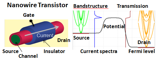
By completing the OMEN Nanowire Lab, you will be able to:
a) understand the operation of nanowire FETs,
b) effect of bandstructure on the carrier transport in nanowire FETs,
c) effect of geometry of nanowire on the drain current characteristics in nanowire FETs
The specific objectives of the OMEN Nanowire Lab are:

Recommended Reading
Following materials introduce the concept of nanowire FETs and the simulation methods that are useful to understand thier characterstics:
- Mark Lundstrom, Nanoscale Transistors for a basic understanding on MOS transistors.
- Joerg Appenzeller, What Promises do Nanotubes and Nanowires Hold for Future Nanoelectronics Applications?
- One-dimensional Materials
- Monica Taba, Investigation of the Electrical Characteristics of Triple-Gate FinFETs and Silicon-Nanowire FETs
- Mark Lundstrom, Nanoscale Transistors: Device Physics, Modeling and Simulation, Springer (Chapter 5)
- Saumitra R. Mehrotra, et al., Threshold voltage
- Mark Lundstrom, Subthreshold conduction
Demo
Theoretical Descriptions
- Mathieu Luisier, et al., Atomistic simulation of nanowires in the sp3d5s* tight-binding formalism: From boundary conditions to strain calculations, Physical Review B 74, 205323, 2006
- Mathieu Luisier, Quantum transport beyond the effective mass approximation, ph.D. thesis, ETH, 2007
- Mathieu Luisier, Quantum Transport for Nanostructures
- Dragica Vasileska, et al., Tight-Binding Bandstructure Calculation Method
Tool Verification
Worked Examples
Homework
Solutions to Exercises
- Solutions to exercises are provided to Instructors ONLY!