Tunneling in an Nanometer-Scaled Transistor
Category
Published on
Abstract
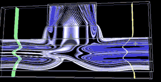
Electrons tunneling through the gate of an ultra-scaled transistor.
 The continued down-scaling of transistors has enabled tremendous advances in consumer electronics. We are reaching the limits where individual transistors or on-off electron valves are only a few nanometers in diameters wide. At these atomic length scales the electrons no longer act like billiard balls but rather like waves. As a result, electrons can tunnel through forbidden device regions, causing additional conduction and heat generation paths. Sophisticated modeling engines that consider a quantum mechanical description of the electrons, an atomistic description of the material, and non-equilibrium electron distributions, are needed for device design and optimization.
The "OMEN_FET" tool on nanoHUB.org enables such device modeling, and allows for the visualization of the electron density in such ultra-scaled structures through 3D volume rendering.
The current density was computed with the OMEN_FET tool and visualized with the nanoVIZ tool on nanoHUB.org.
Credits
Purdue University
References
- Transistor Design:
Neerav Kharche, Gerhard Klimeck, Dae-Hyun Kim, Jesús. A. del Alamo, and Mathieu Luisier, "Performance Analysis of Ultra-Scaled InAs HEMTs", IEDM 2009, Dec. 7-9, 2009. - nanoVIZ:
Wei Qiao, Michael Mclennan, Rick Kennell, David Ebert, and Gerhard Klimeck, "Hub-based Simulation and Graphics Hardware Accelerated Visualization for Nanotechnology Applications", IEEE Transactions on Visualization and Computer Graphics, Vol. 12, pg. 1061-1068 (2006). - nanoHUB.org:
Alejandro Strachan, Gerhard Klimeck, Mark S. Lundstrom, "Cyber-Enabled Simulations in Nanoscale Science and Engineering", Computing in Science and Engineering, Vol. 12, pg: 12-17 (2010). (available on nanoHUB.org) - OMEN_FET tool on nanoHUB.org:
Neerav Kharche; Mathieu Luisier; George A. Howlett; Gerhard Klimeck; Mehdi Salmani Jelodar (2009), "OMEN_FET," DOI: 10254/nanohub-r6637.5.
Cite this work
Researchers should cite this work as follows: