Atomistic Modeling of Nano Devices: From Qubits to Transistors
 Rajib Rahman obtained his PhD degree in Electrical and Computer Engineering from Purdue University in 2009 in the area of computational nanoelectronics. Subsequently, he was a postdoctoral fellow in Sandia National Laboratories in the Silicon Quantum Information Science and Technology group. Since 2012, he has been employed as a Research Assistant Professor in the Network for Computational Nanotechnology (NCN) at Purdue. Rajib develops and employs atomistic simulation methods to model spin qubits in semiconductors taking into account their complex interaction with the environment in the form of electron-electron, electron-phonon, and magnetic interactions. He collaborates with leading experimental groups from Australia, Netherlands, and USA in the field of silicon quantum computing. At Purdue, Rajib also works on atomistic transport simulations of energy efficient transistors in emerging 2D materials.
Atomistic Modeling of Nano Devices: From Qubits to Transistors


-
 1. Atomistic Modeling of Nano Dev…
0
00:00/00:00
1. Atomistic Modeling of Nano Dev…
0
00:00/00:00 -
 2. The Future of Electronics?
26.893560226893563
00:00/00:00
2. The Future of Electronics?
26.893560226893563
00:00/00:00 -
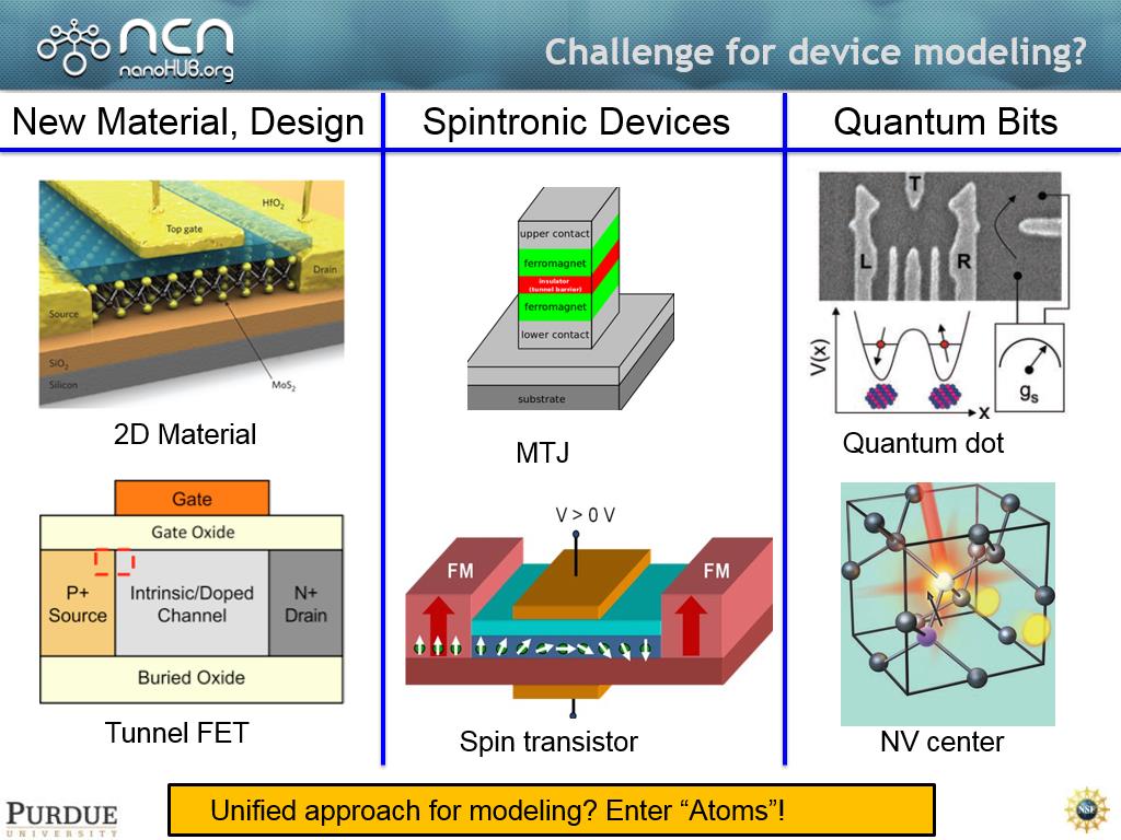 3. Challenge for device modeling?
79.946613279946618
00:00/00:00
3. Challenge for device modeling?
79.946613279946618
00:00/00:00 -
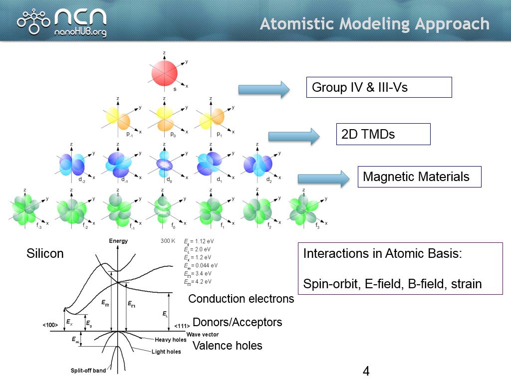 4. Atomistic Modeling Approach
123.82382382382383
00:00/00:00
4. Atomistic Modeling Approach
123.82382382382383
00:00/00:00 -
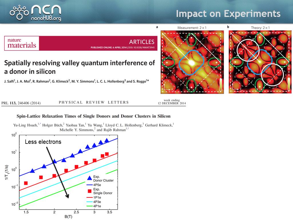
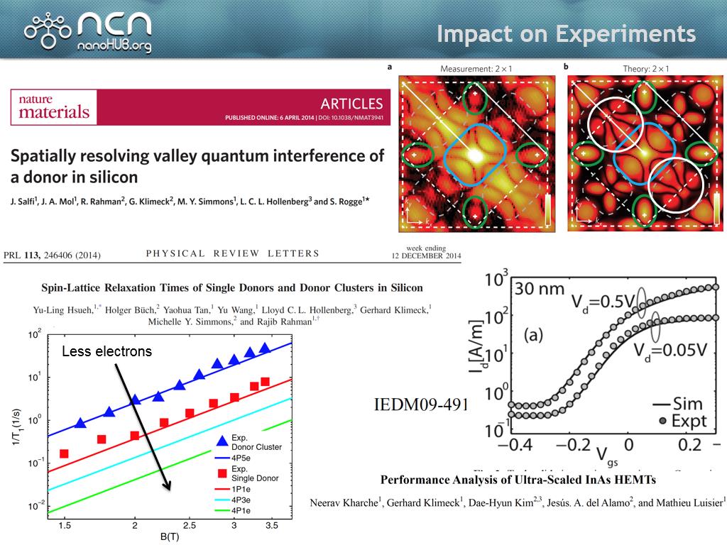
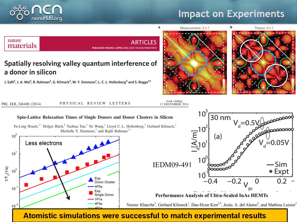 5. Impact on Experiments
192.32565899232566
00:00/00:00
5. Impact on Experiments
192.32565899232566
00:00/00:00 -
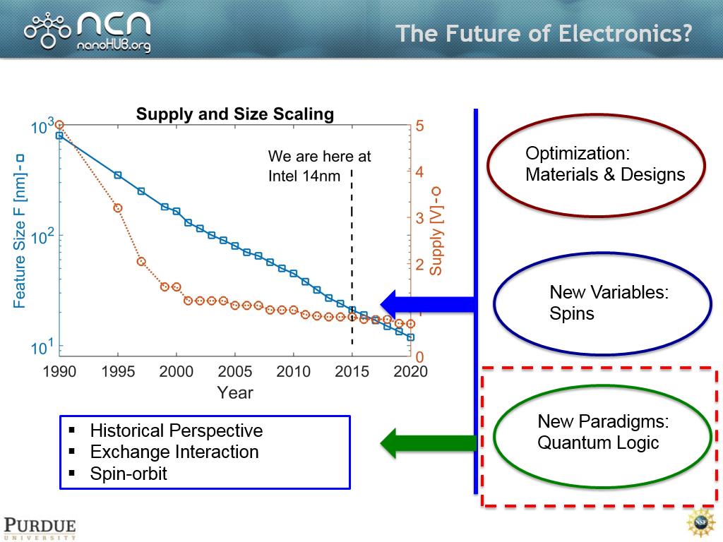 6. The Future of Electronics?
347.74774774774778
00:00/00:00
6. The Future of Electronics?
347.74774774774778
00:00/00:00 -
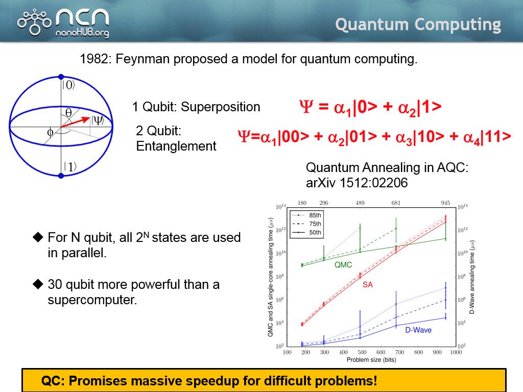 7. Quantum Computing
368.70203536870207
00:00/00:00
7. Quantum Computing
368.70203536870207
00:00/00:00 -
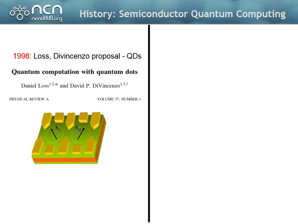
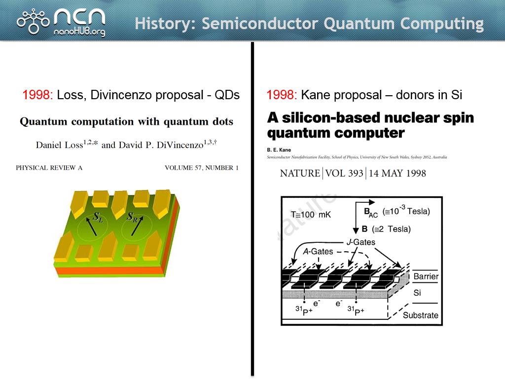
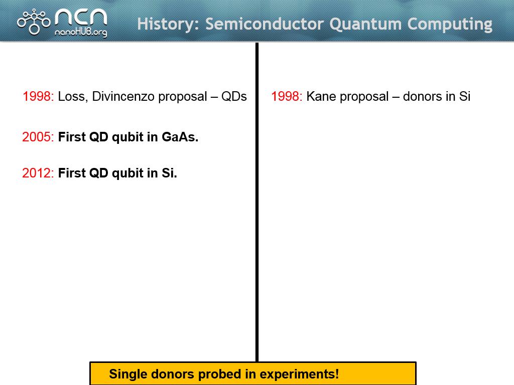
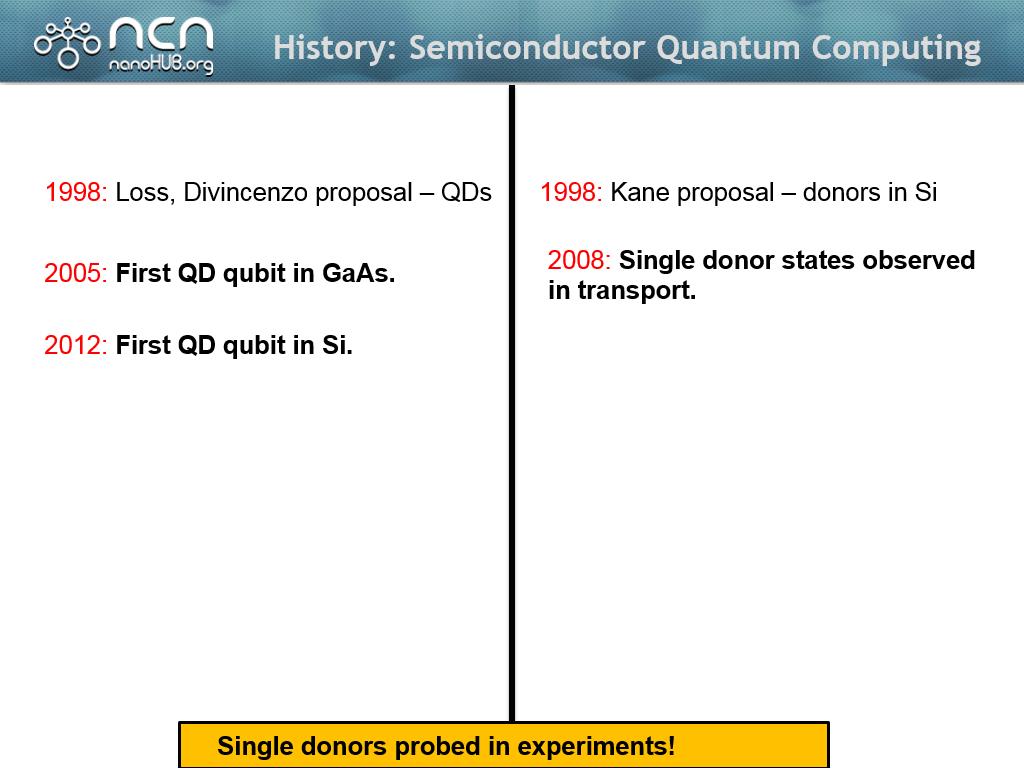
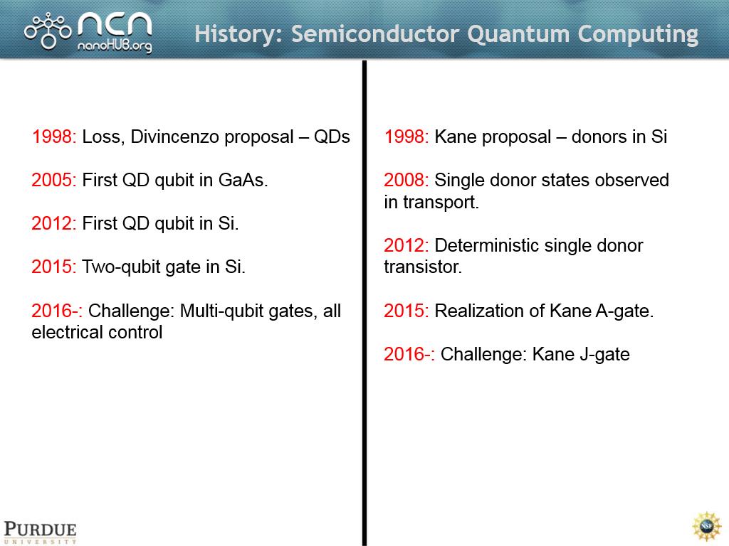
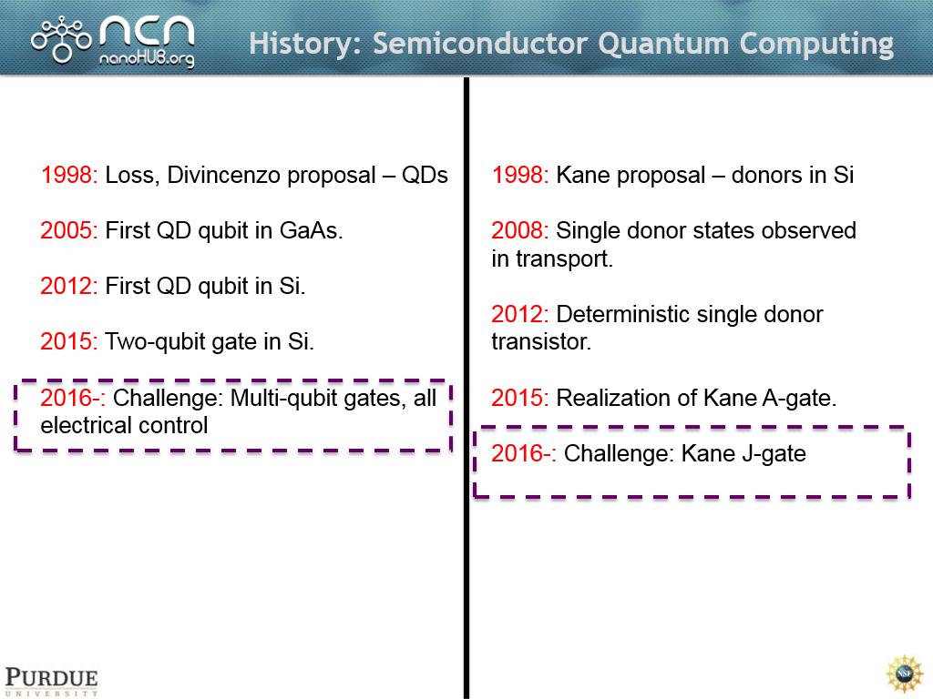
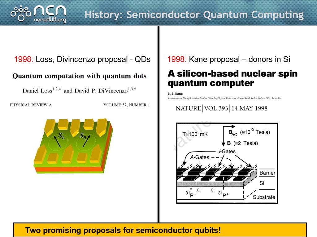 8. History: Semiconductor Quantum…
472.77277277277278
00:00/00:00
8. History: Semiconductor Quantum…
472.77277277277278
00:00/00:00 -
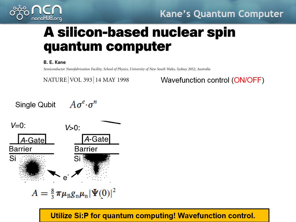
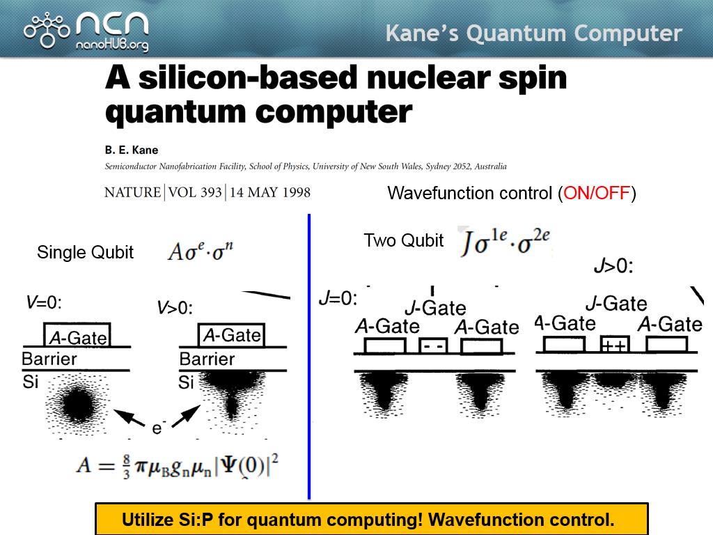 9. Kane's Quantum Computer
551.45145145145148
00:00/00:00
9. Kane's Quantum Computer
551.45145145145148
00:00/00:00 -
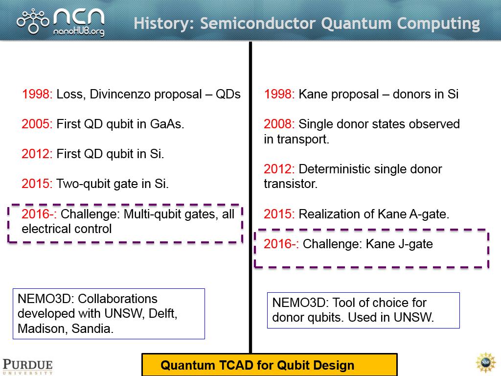
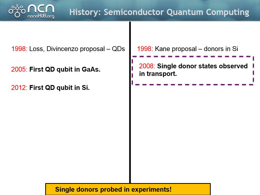 10. History: Semiconductor Quantum…
664.63129796463136
00:00/00:00
10. History: Semiconductor Quantum…
664.63129796463136
00:00/00:00 -
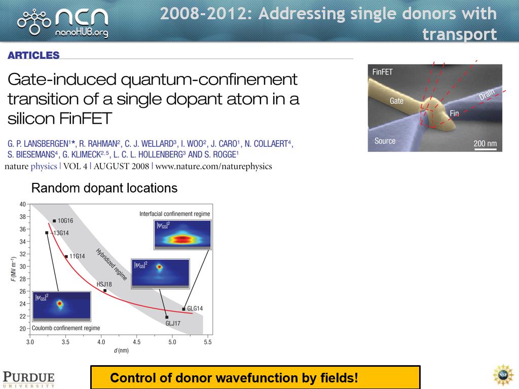
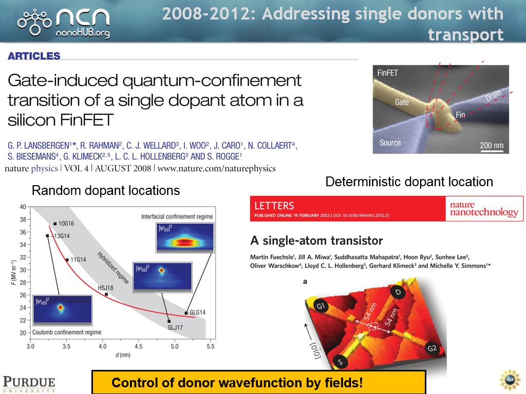 11. 2008-2012: Addressing single d…
727.19386052719392
00:00/00:00
11. 2008-2012: Addressing single d…
727.19386052719392
00:00/00:00 -
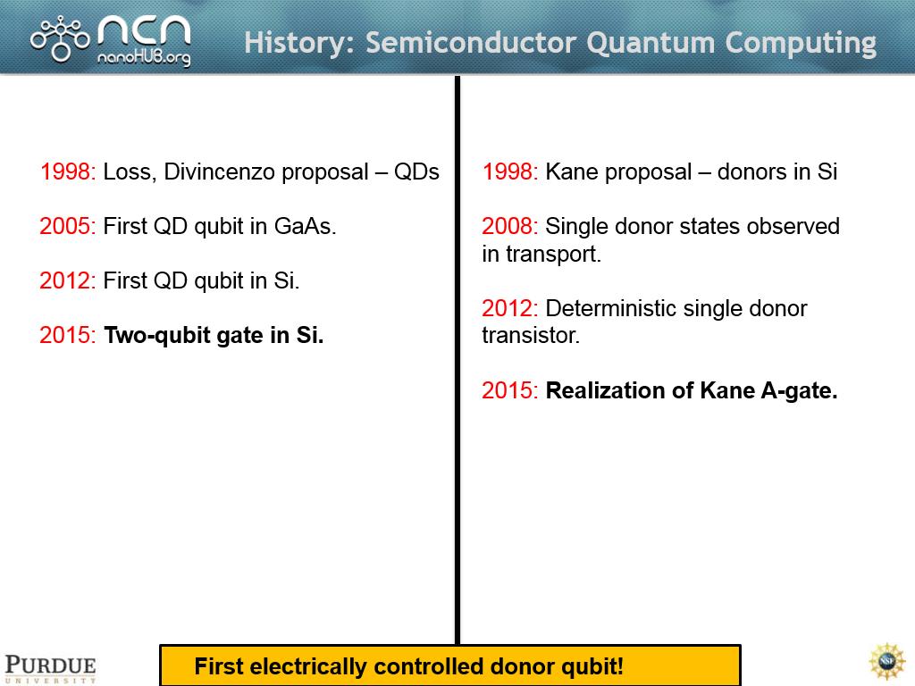
 12. History: Semiconductor Quantum…
1041.9085752419087
00:00/00:00
12. History: Semiconductor Quantum…
1041.9085752419087
00:00/00:00 -
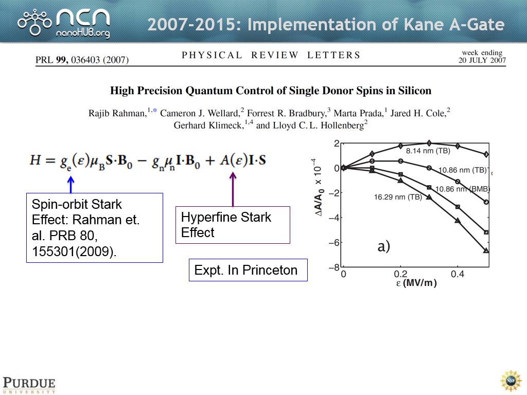
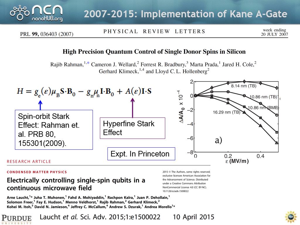
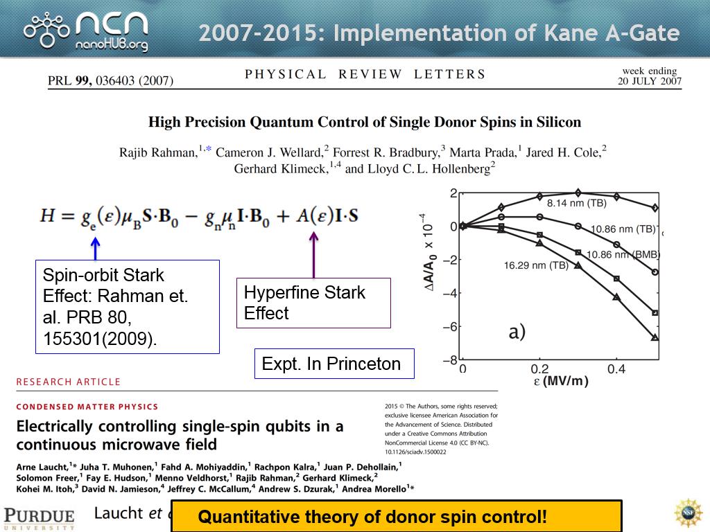 13. 2007-2015: Implementation of K…
1065.7991324657992
00:00/00:00
13. 2007-2015: Implementation of K…
1065.7991324657992
00:00/00:00 -
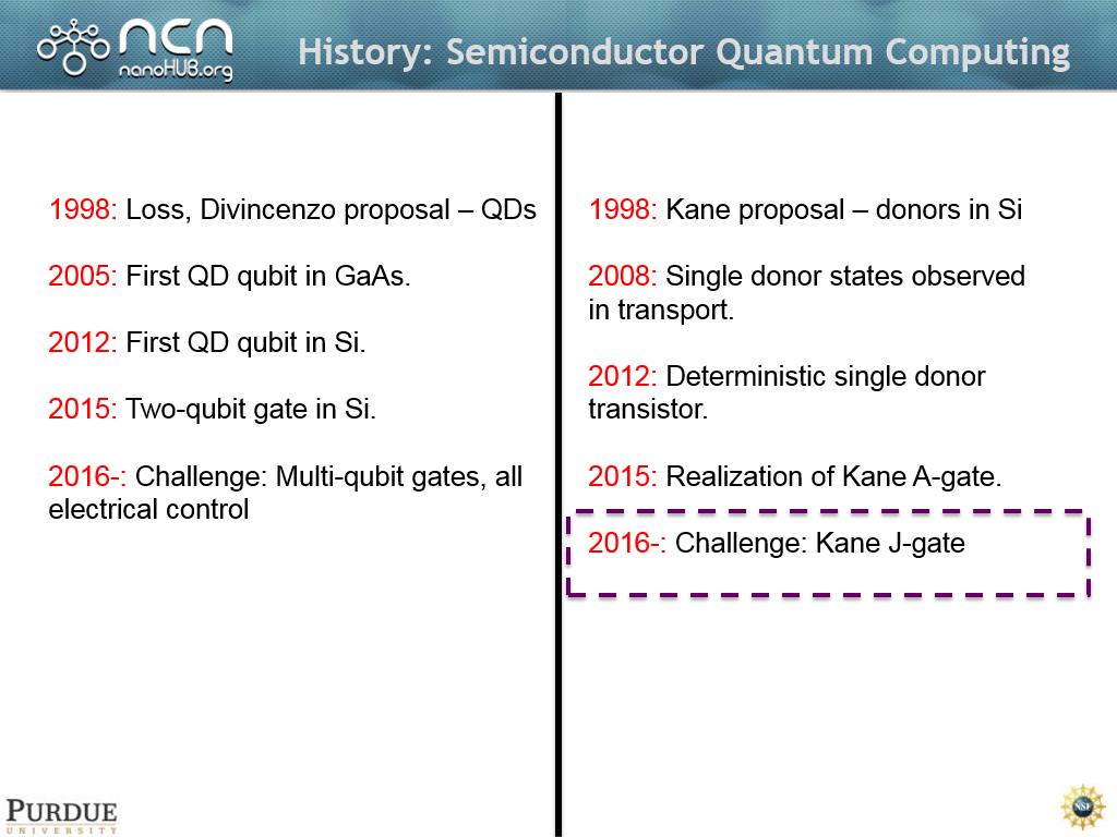
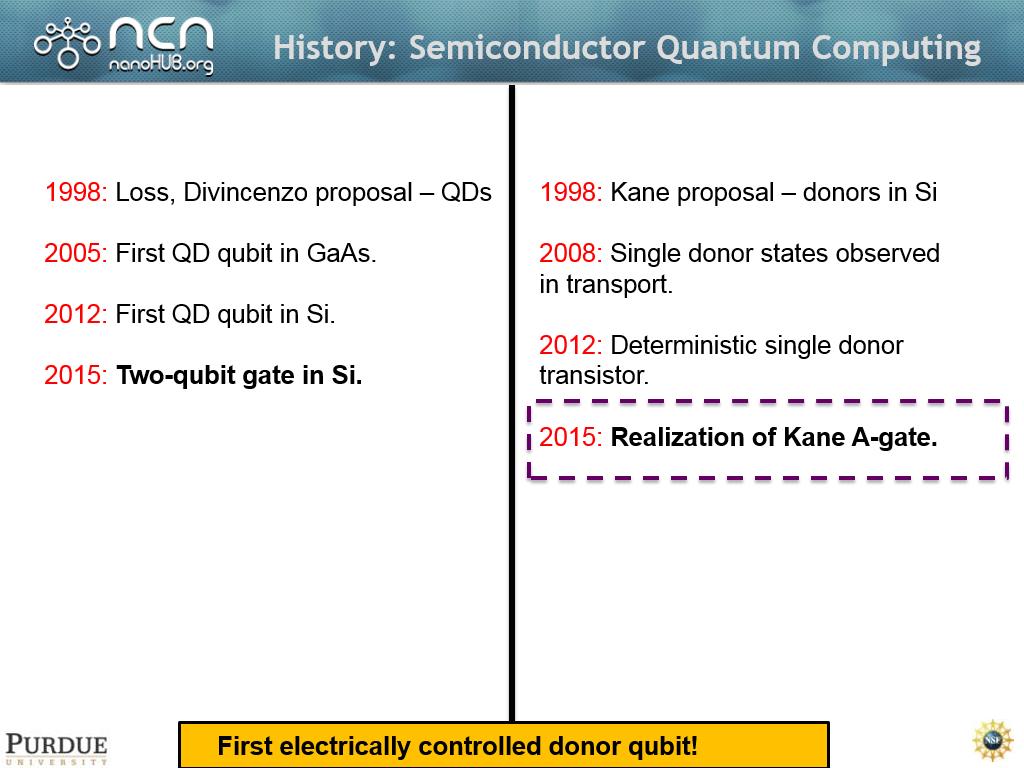
 14. History: Semiconductor Quantum…
1175.1418084751419
00:00/00:00
14. History: Semiconductor Quantum…
1175.1418084751419
00:00/00:00 -
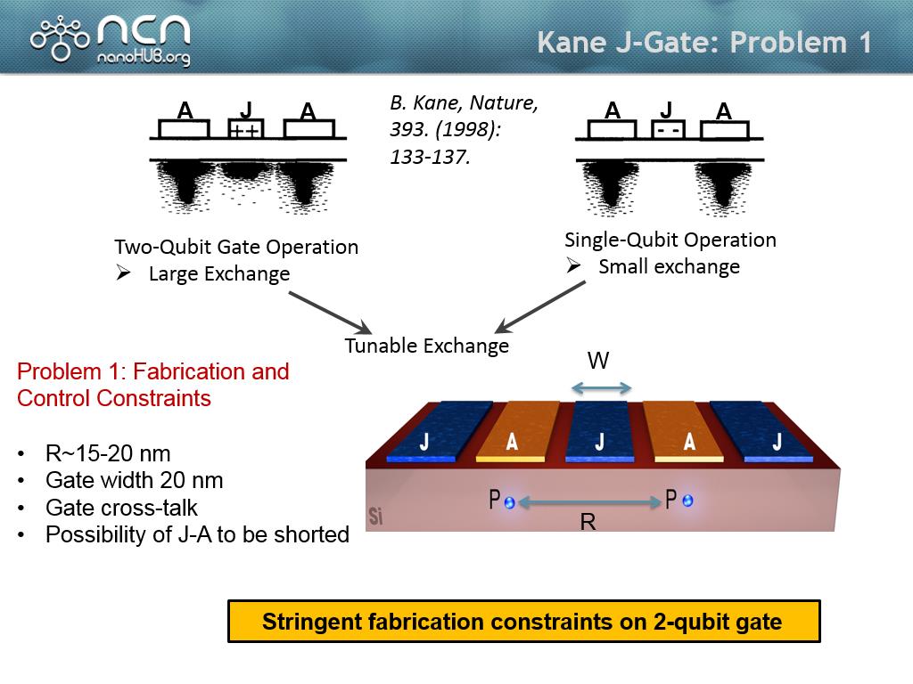 15. Kane J-Gate: Problem 1
1259.2926259592928
00:00/00:00
15. Kane J-Gate: Problem 1
1259.2926259592928
00:00/00:00 -
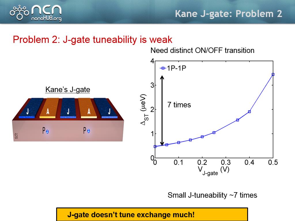 16. Kane J-gate: Problem 2
1318.4851518184853
00:00/00:00
16. Kane J-gate: Problem 2
1318.4851518184853
00:00/00:00 -
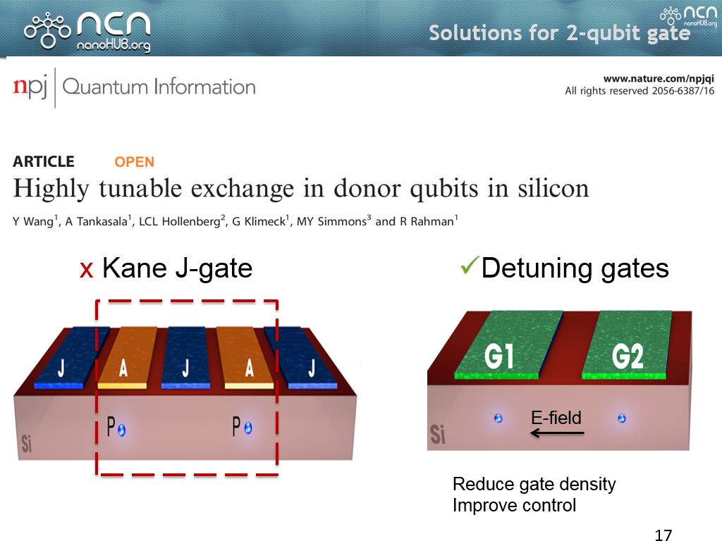 17. Solutions for 2-qubit gate
1347.3473473473473
00:00/00:00
17. Solutions for 2-qubit gate
1347.3473473473473
00:00/00:00 -
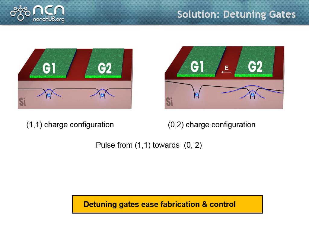 18. Solution: Detuning Gates
1381.4481147814481
00:00/00:00
18. Solution: Detuning Gates
1381.4481147814481
00:00/00:00 -
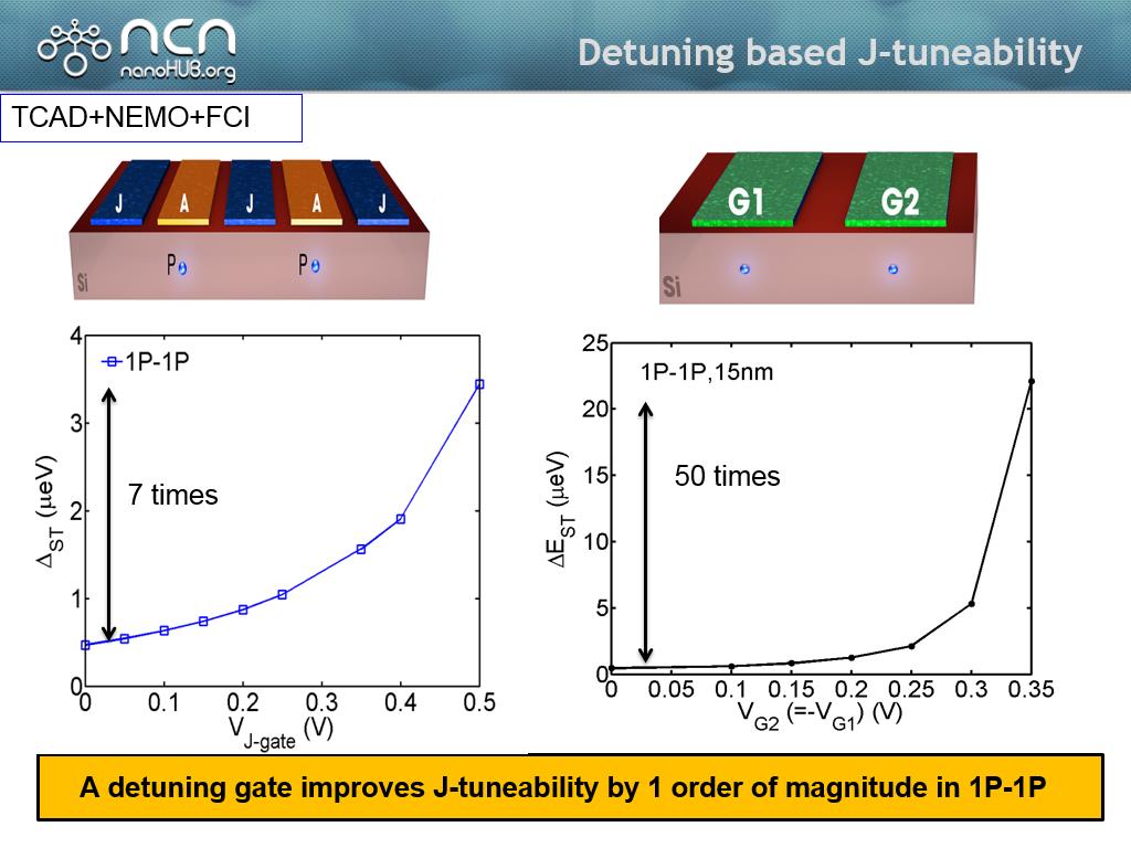 19. Detuning based J-tuneability
1422.9896563229897
00:00/00:00
19. Detuning based J-tuneability
1422.9896563229897
00:00/00:00 -
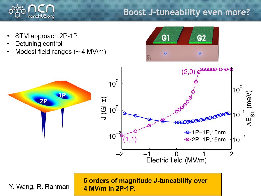 20. Boost J-tuneability even more?
1447.1805138471805
00:00/00:00
20. Boost J-tuneability even more?
1447.1805138471805
00:00/00:00 -
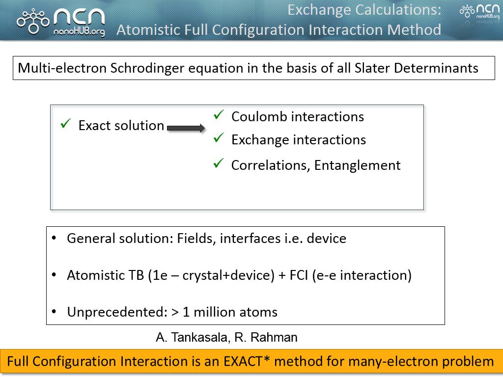 21. Exchange Calculations: Atomist…
1520.2535869202536
00:00/00:00
21. Exchange Calculations: Atomist…
1520.2535869202536
00:00/00:00 -
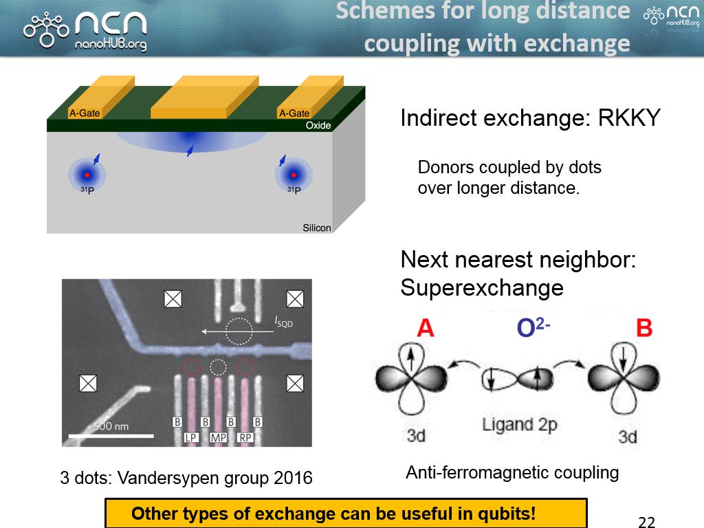 22. Schemes for long distance coup…
1580.7807807807808
00:00/00:00
22. Schemes for long distance coup…
1580.7807807807808
00:00/00:00 -
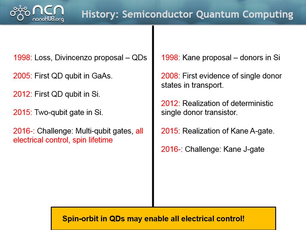
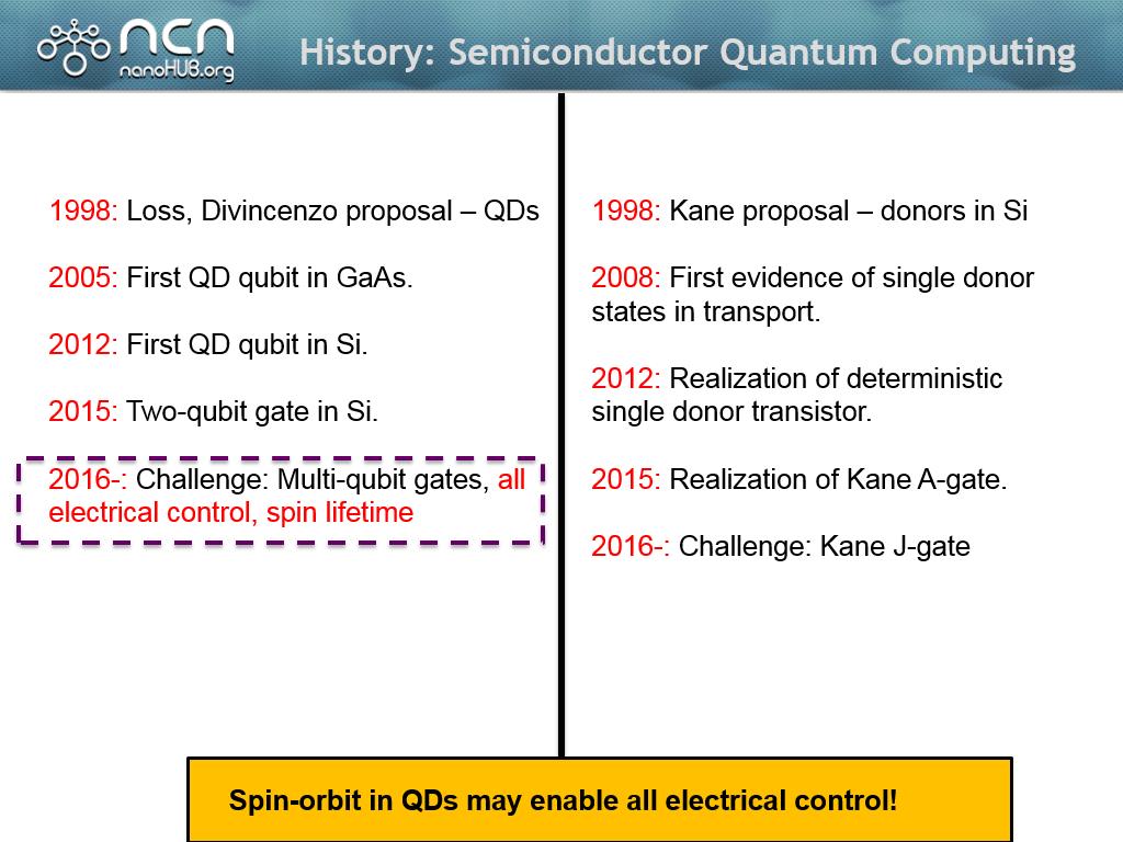 23. History: Semiconductor Quantum…
1669.4361027694363
00:00/00:00
23. History: Semiconductor Quantum…
1669.4361027694363
00:00/00:00 -
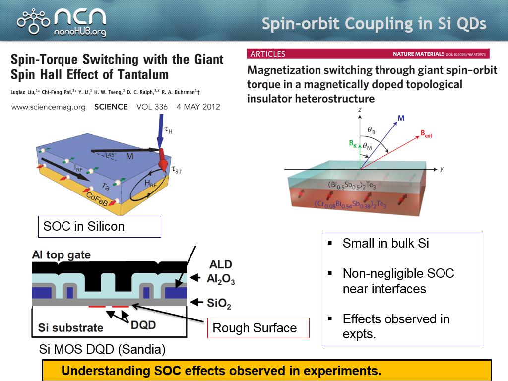 24. Spin-orbit Coupling in Si QDs
1687.6543209876543
00:00/00:00
24. Spin-orbit Coupling in Si QDs
1687.6543209876543
00:00/00:00 -
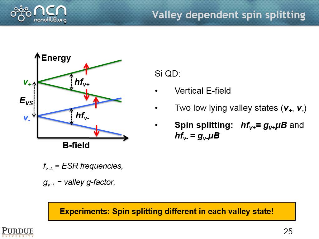 25. Valley dependent spin splittin…
1904.2375709042376
00:00/00:00
25. Valley dependent spin splittin…
1904.2375709042376
00:00/00:00 -
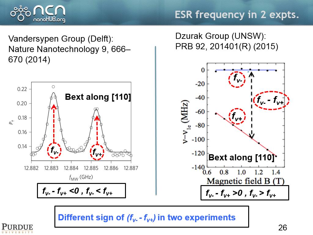
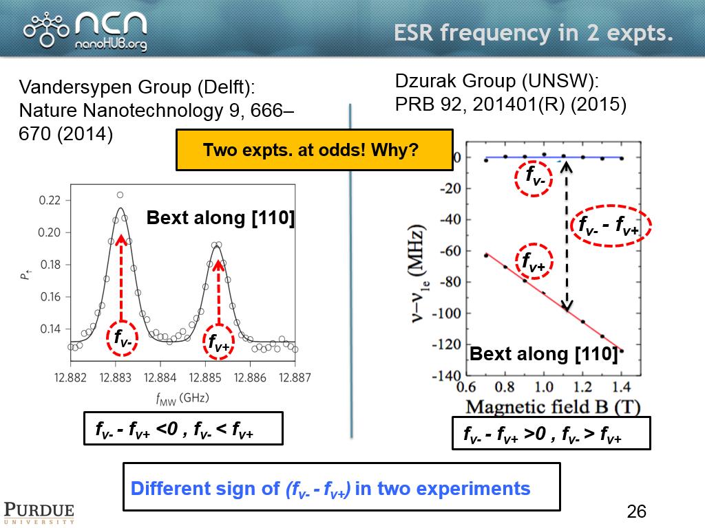 26. ESR frequency in 2 expts.
1963.963963963964
00:00/00:00
26. ESR frequency in 2 expts.
1963.963963963964
00:00/00:00 -
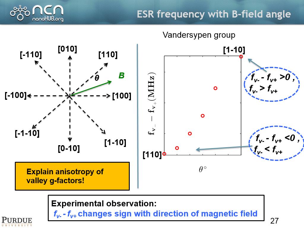 27. ESR frequency with B-field ang…
2005.8725392058727
00:00/00:00
27. ESR frequency with B-field ang…
2005.8725392058727
00:00/00:00 -
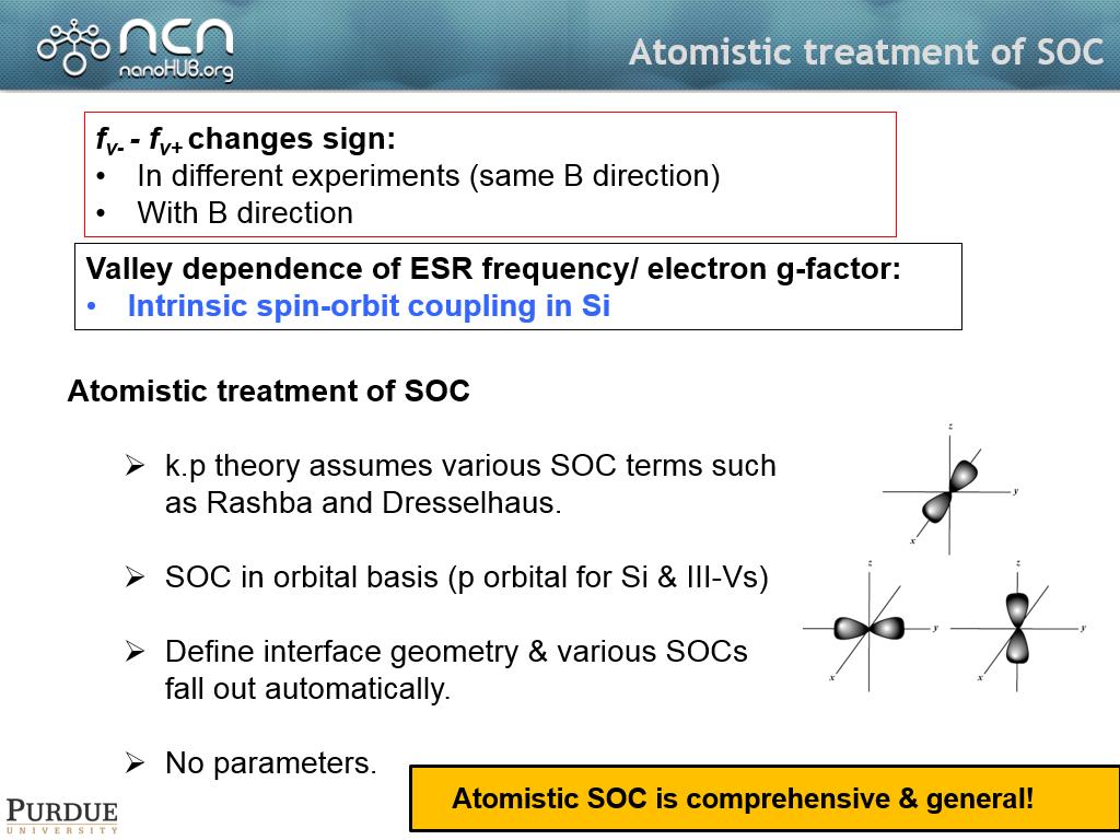 28. Atomistic treatment of SOC
2035.201868535202
00:00/00:00
28. Atomistic treatment of SOC
2035.201868535202
00:00/00:00 -
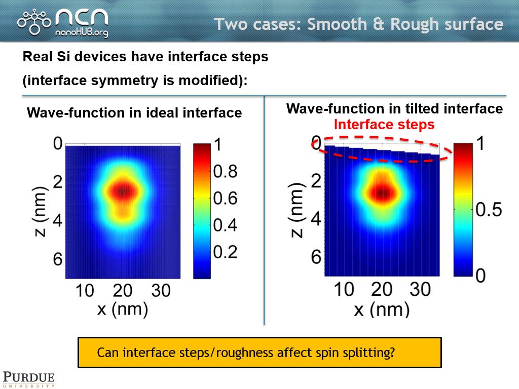 29. Two cases: Smooth & Rough surf…
2097.2305638972307
00:00/00:00
29. Two cases: Smooth & Rough surf…
2097.2305638972307
00:00/00:00 -
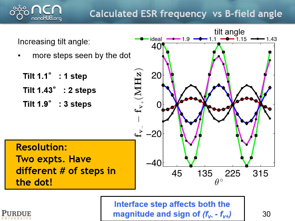
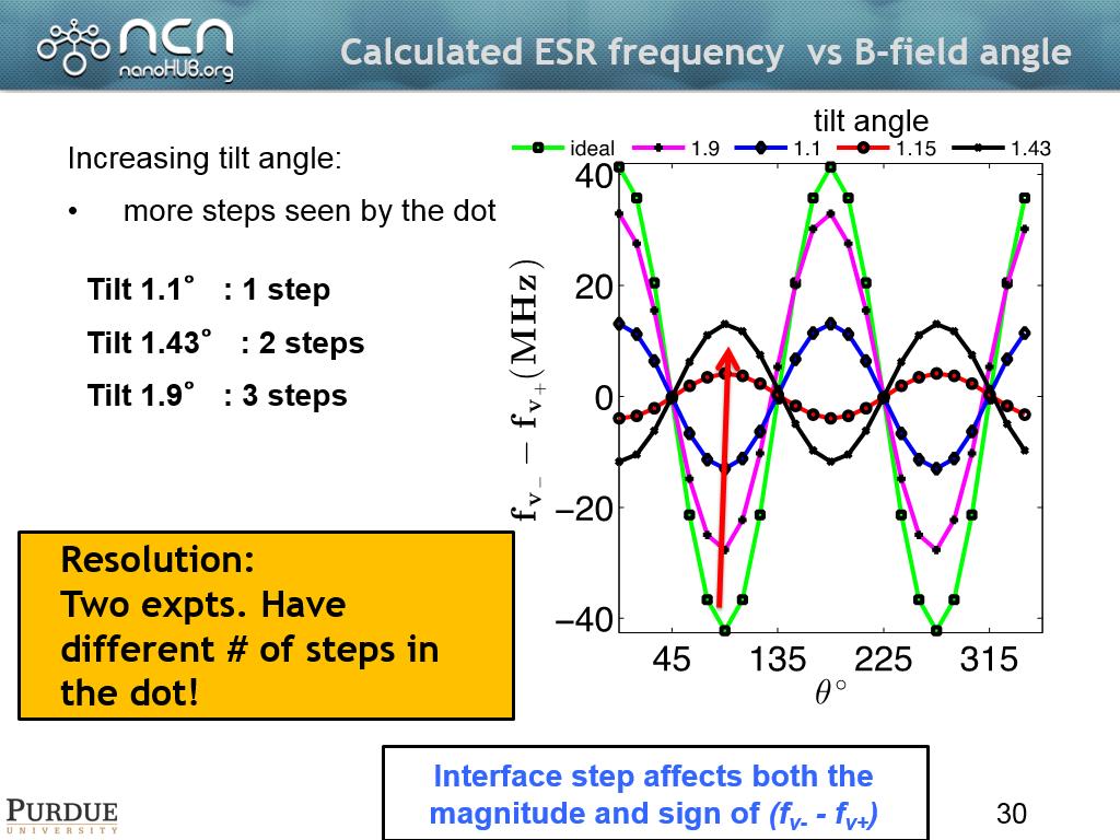 30. Calculated ESR frequency vs B-…
2130.8975642308978
00:00/00:00
30. Calculated ESR frequency vs B-…
2130.8975642308978
00:00/00:00 -
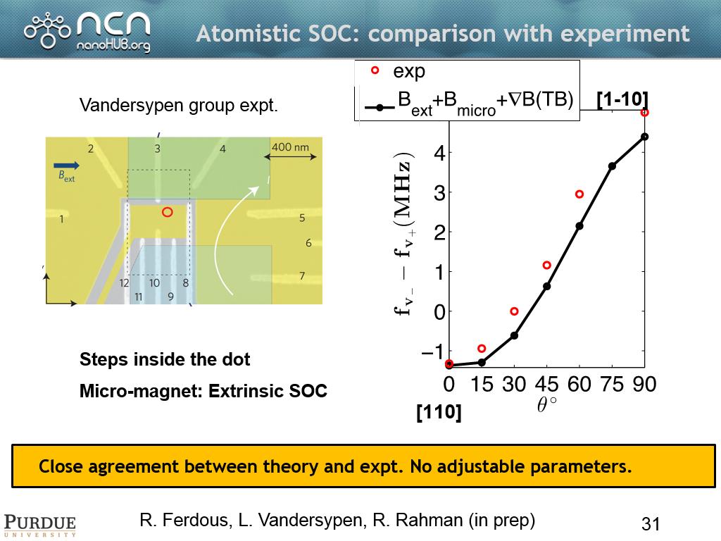 31. Atomistic SOC: comparison with…
2187.8878878878882
00:00/00:00
31. Atomistic SOC: comparison with…
2187.8878878878882
00:00/00:00 -
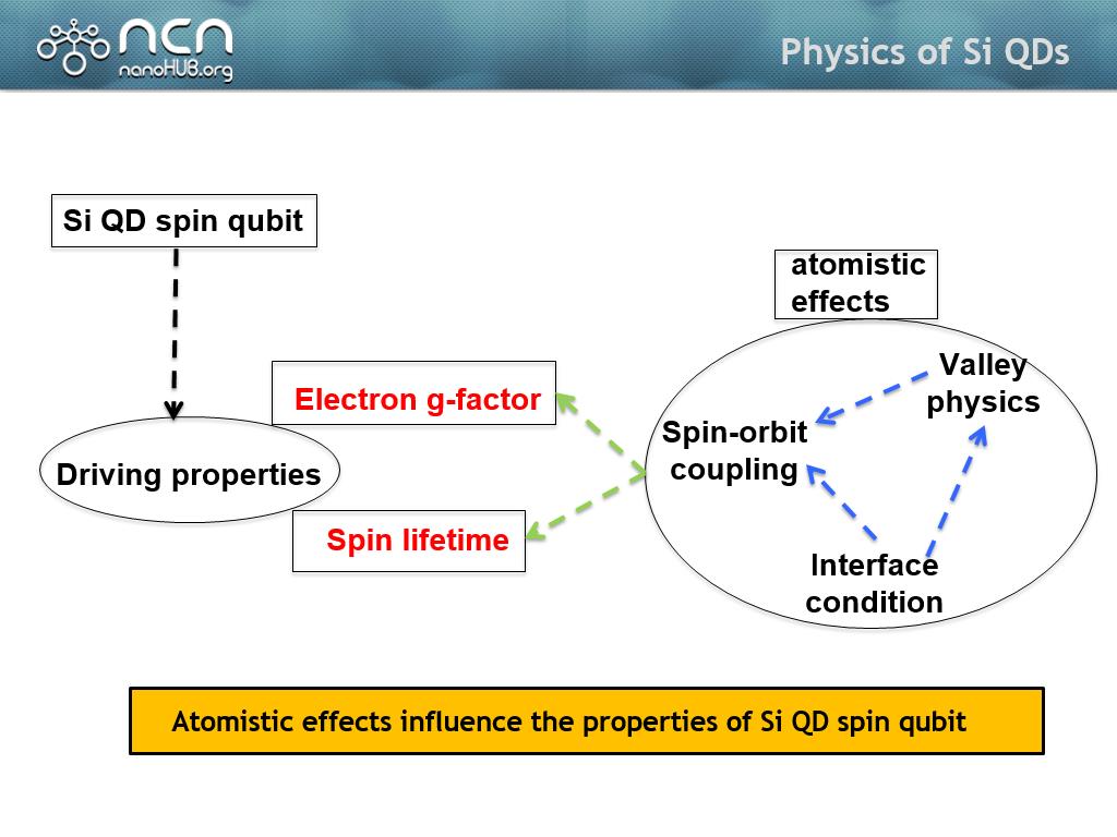 32. Physics of Si QDs
2214.3810477143811
00:00/00:00
32. Physics of Si QDs
2214.3810477143811
00:00/00:00 -
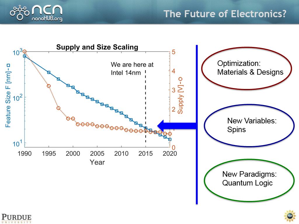
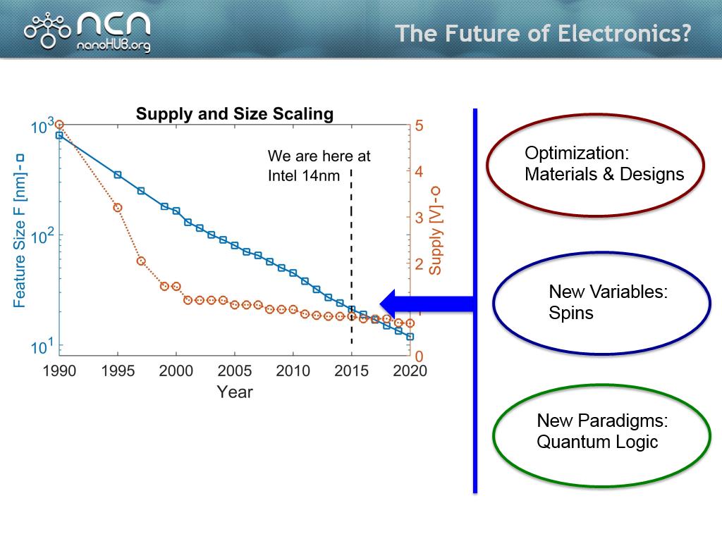
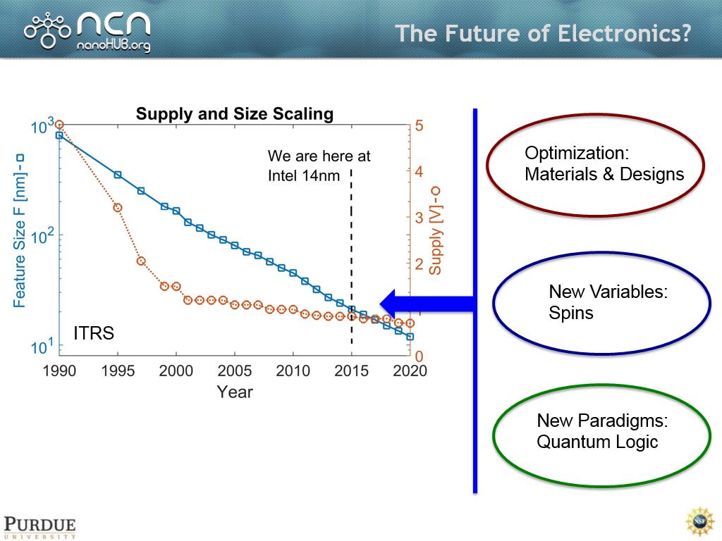
 33. The Future of Electronics?
2249.5829162495829
00:00/00:00
33. The Future of Electronics?
2249.5829162495829
00:00/00:00 -
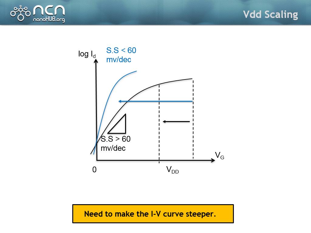 34. Vdd Scaling
2423.8571905238573
00:00/00:00
34. Vdd Scaling
2423.8571905238573
00:00/00:00 -
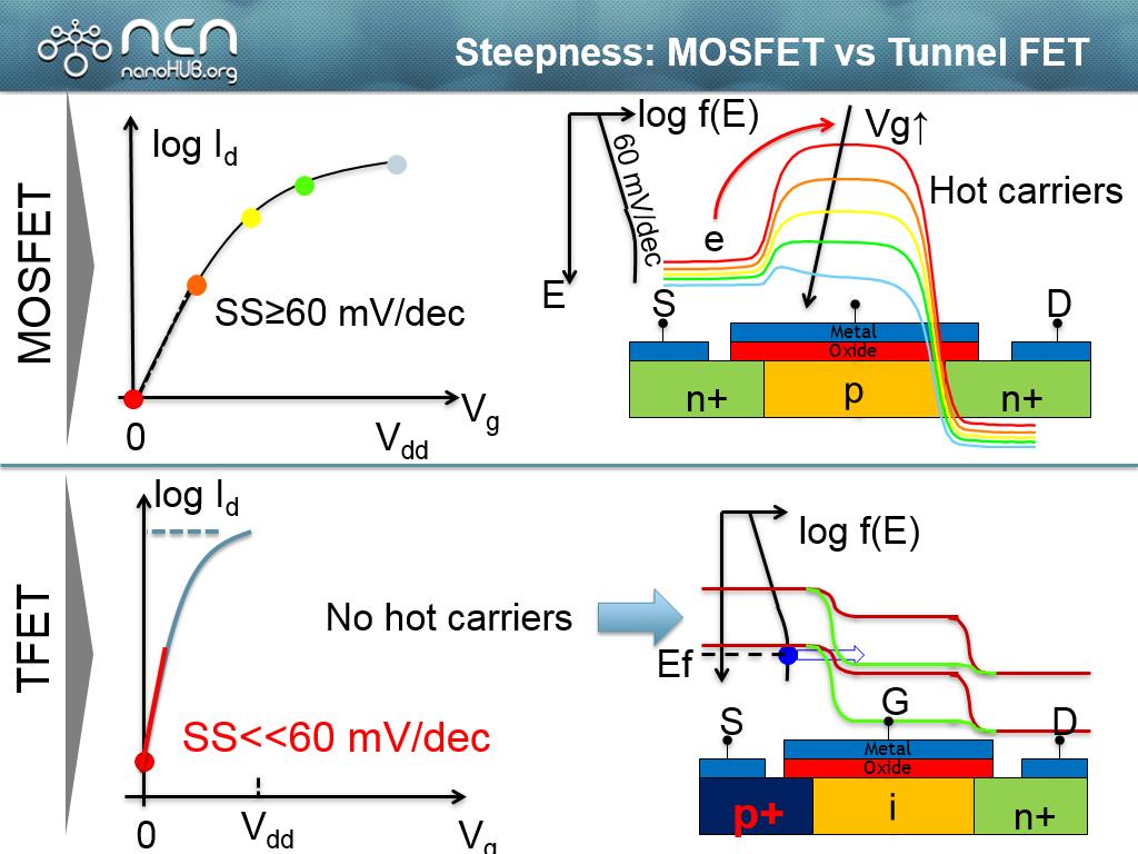 35. Steepness: MOSFET vs Tunnel FE…
2443.677010343677
00:00/00:00
35. Steepness: MOSFET vs Tunnel FE…
2443.677010343677
00:00/00:00 -
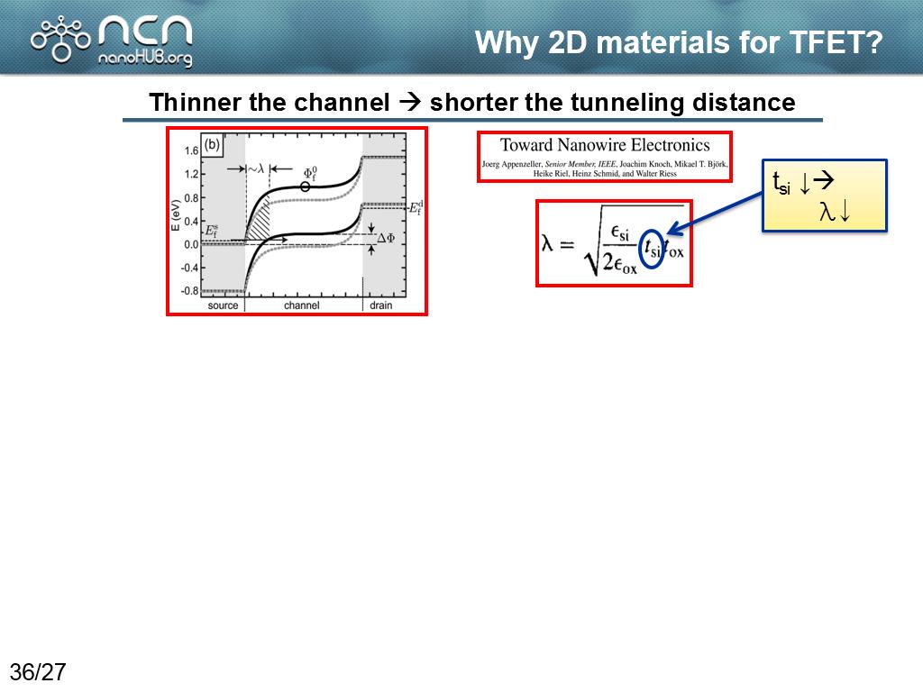
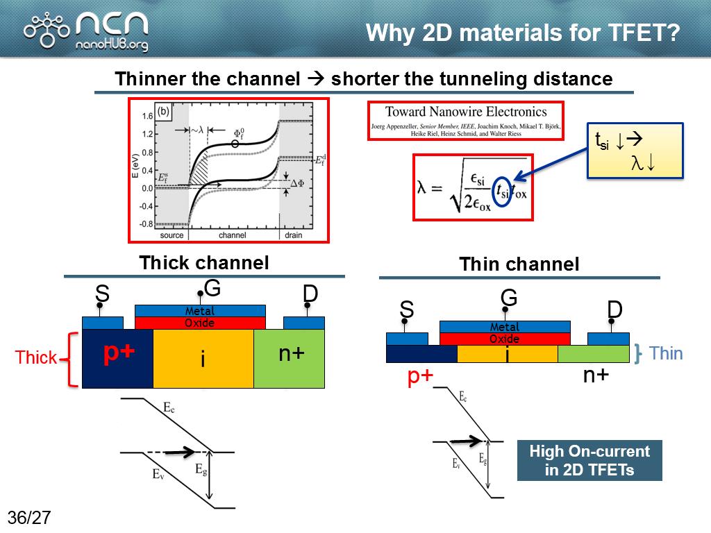
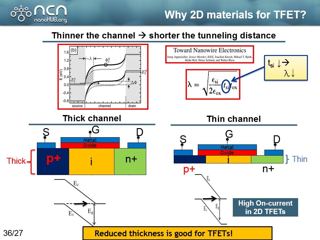 36. Why 2D materials for TFET?
2478.3783783783783
00:00/00:00
36. Why 2D materials for TFET?
2478.3783783783783
00:00/00:00 -
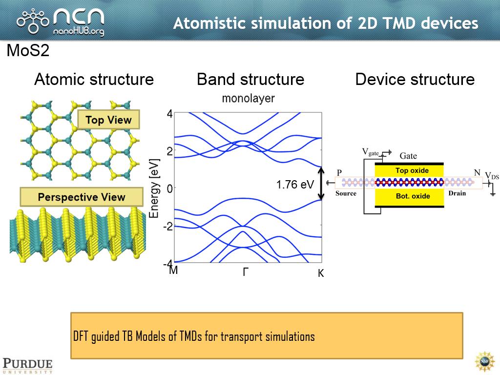 37. Atomistic simulation of 2D TMD…
2542.475809142476
00:00/00:00
37. Atomistic simulation of 2D TMD…
2542.475809142476
00:00/00:00 -
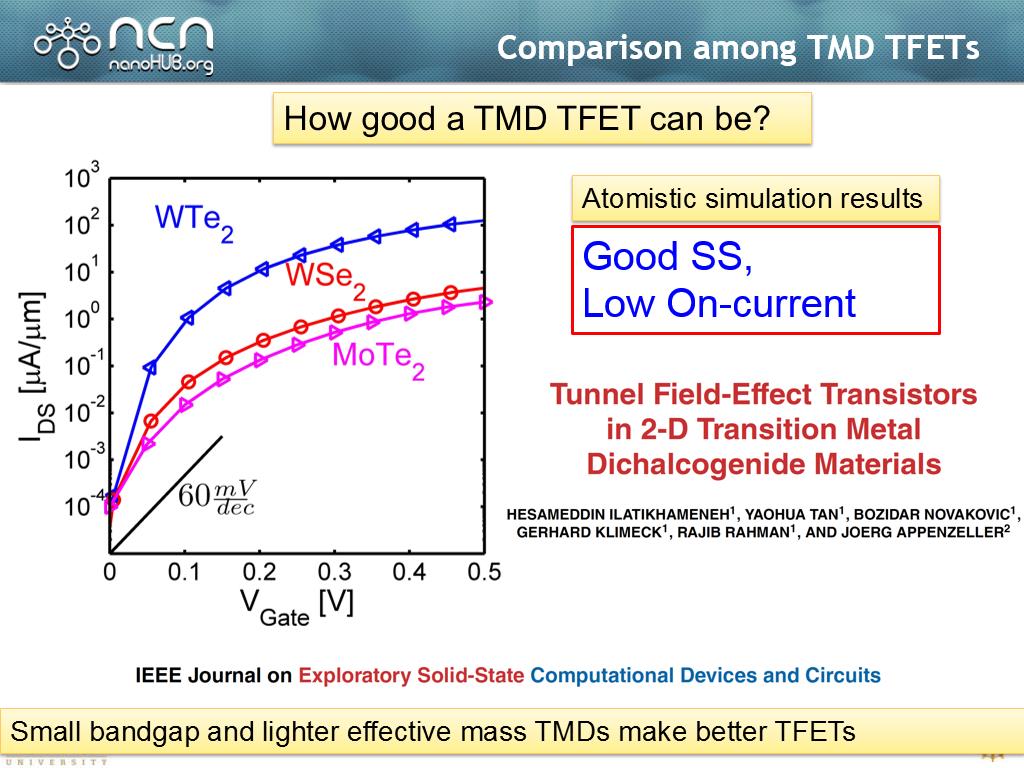 38. Comparison among TMD TFETs
2569.3360026693363
00:00/00:00
38. Comparison among TMD TFETs
2569.3360026693363
00:00/00:00 -
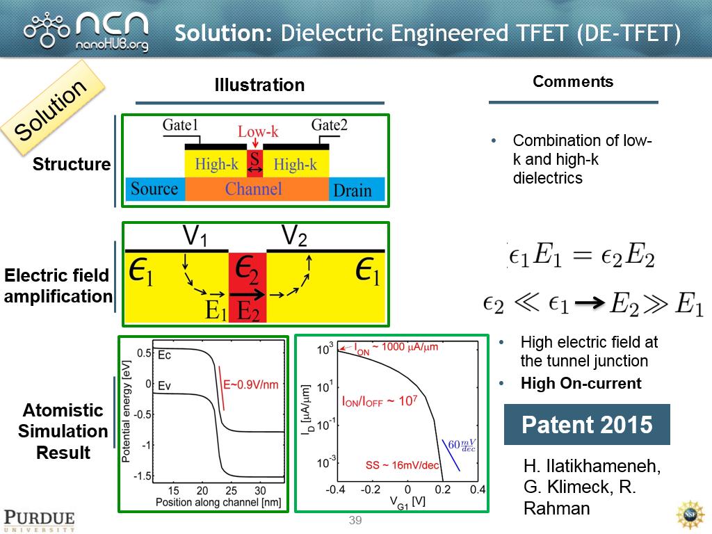 39. Solution: Dielectric Engineere…
2597.6643309976644
00:00/00:00
39. Solution: Dielectric Engineere…
2597.6643309976644
00:00/00:00 -
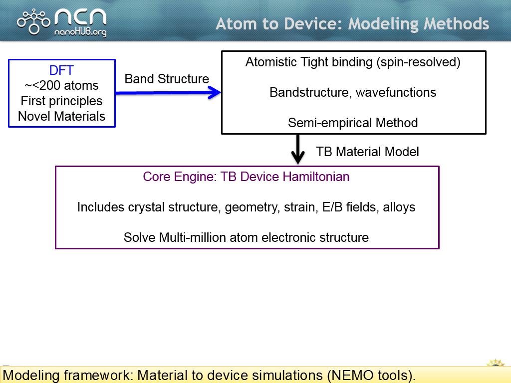
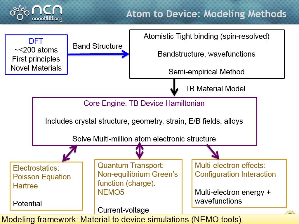 40. Atom to Device: Modeling Metho…
2664.5311978645314
00:00/00:00
40. Atom to Device: Modeling Metho…
2664.5311978645314
00:00/00:00 -
 41. "Atom to Device" Approach in S…
2760.4270937604274
00:00/00:00
41. "Atom to Device" Approach in S…
2760.4270937604274
00:00/00:00 -
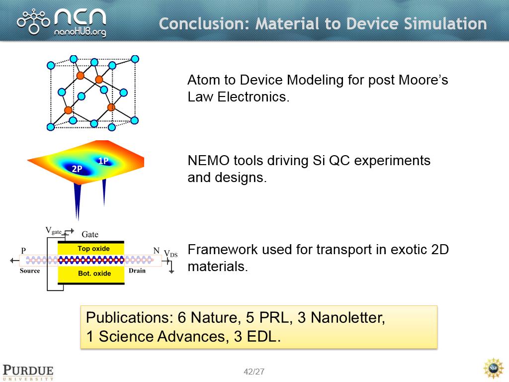 42. Conclusion: Material to Device…
2876.0093426760095
00:00/00:00
42. Conclusion: Material to Device…
2876.0093426760095
00:00/00:00