NEMO5 and 2D Materials: Tuning Bandstructures, Wave Functions and Electrostatic Screening
NEMO5 and 2D Materials: Tuning Bandstructures, Wave Functions and Electrostatic Screening


-
 1. NEMO5 and 2D materials: tuning…
0
00:00/00:00
1. NEMO5 and 2D materials: tuning…
0
00:00/00:00 -
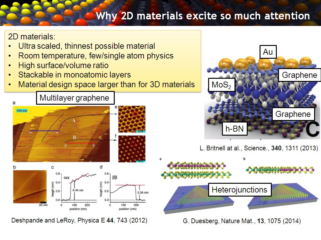 2. Why 2D materials excite so muc…
39.406072739406078
00:00/00:00
2. Why 2D materials excite so muc…
39.406072739406078
00:00/00:00 -
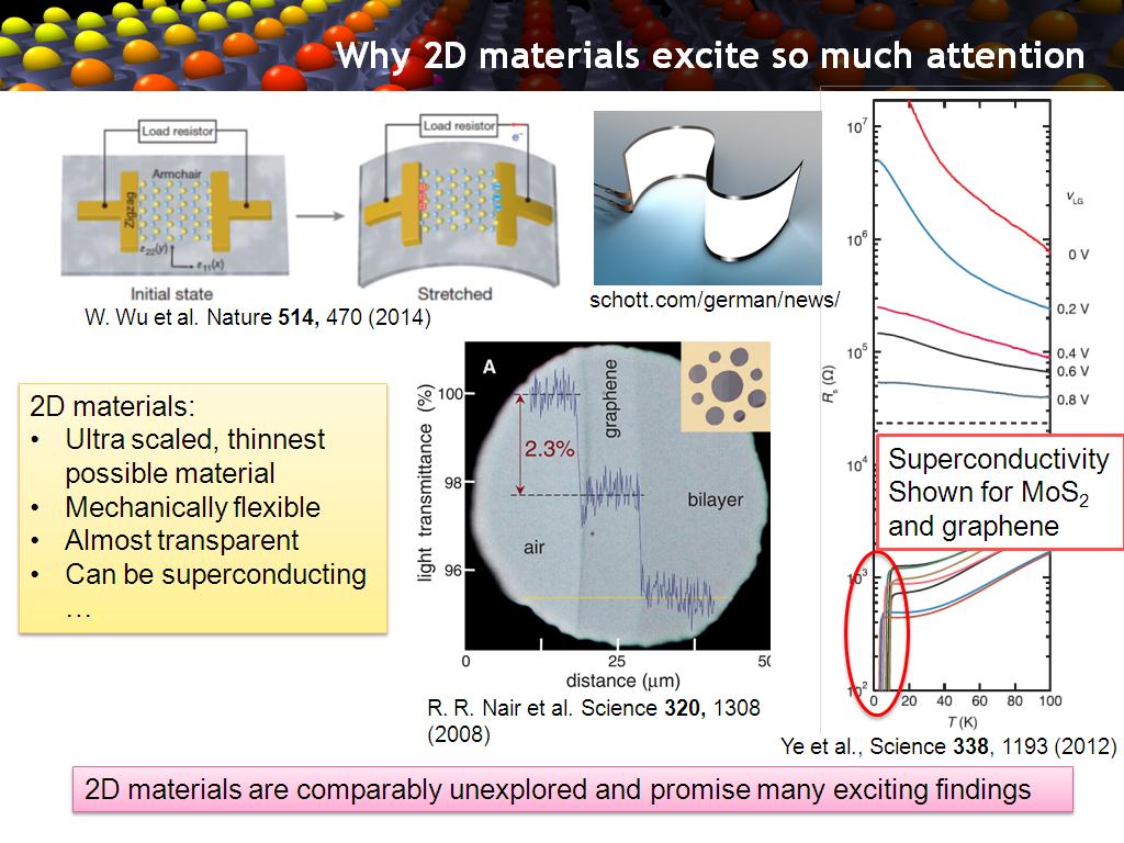 3. Why 2D materials excite so muc…
124.82482482482483
00:00/00:00
3. Why 2D materials excite so muc…
124.82482482482483
00:00/00:00 -
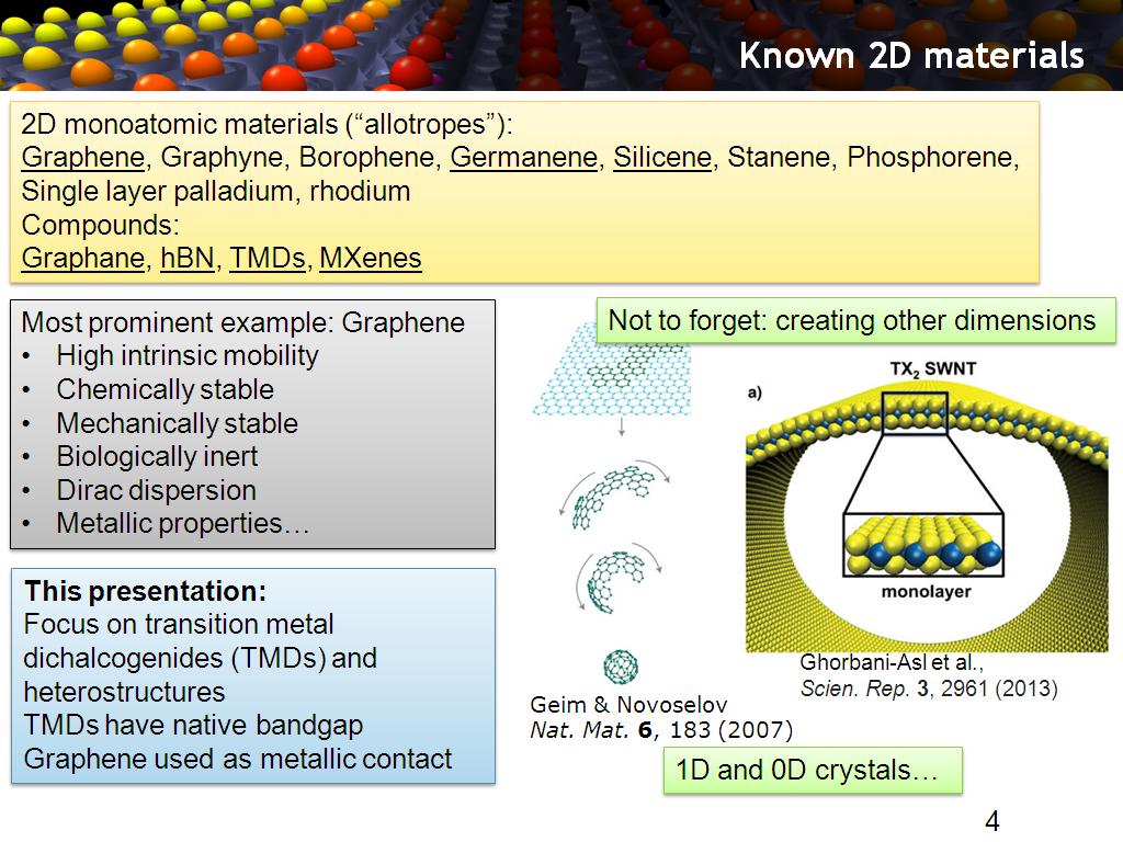 4. Known 2D materials
187.72105438772107
00:00/00:00
4. Known 2D materials
187.72105438772107
00:00/00:00 -
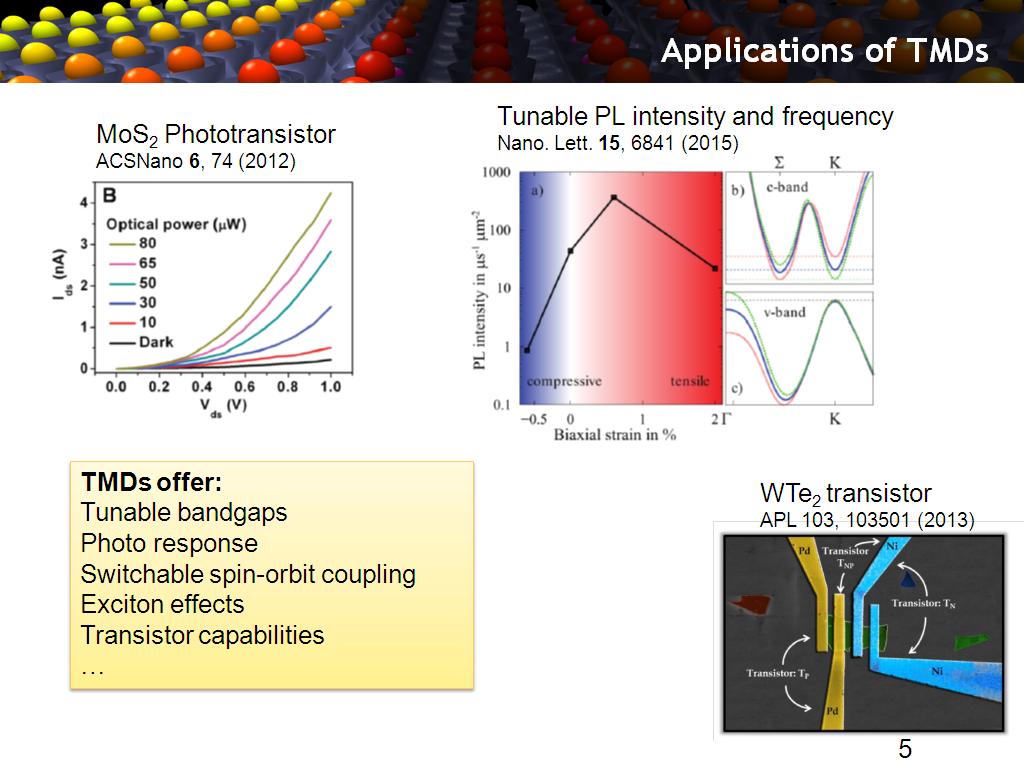 5. Applications of TMDs
264.16416416416416
00:00/00:00
5. Applications of TMDs
264.16416416416416
00:00/00:00 -
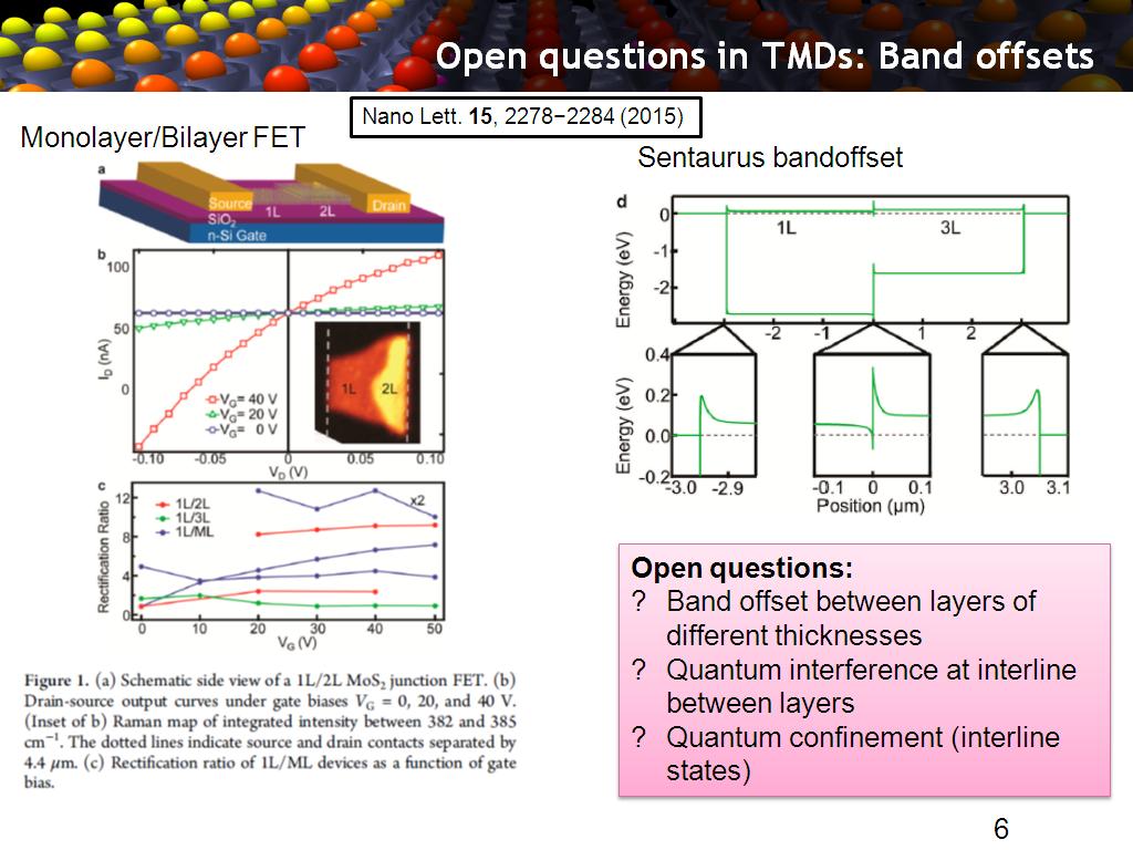 6. Open questions in TMDs: Band o…
297.997997997998
00:00/00:00
6. Open questions in TMDs: Band o…
297.997997997998
00:00/00:00 -
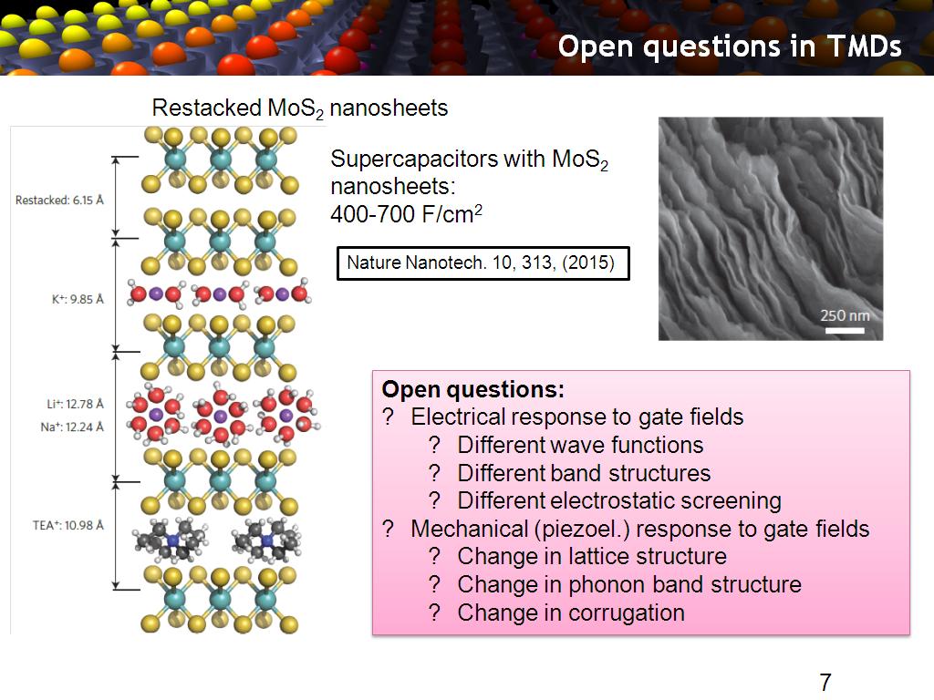 7. Open questions in TMDs
340.77410744077412
00:00/00:00
7. Open questions in TMDs
340.77410744077412
00:00/00:00 -
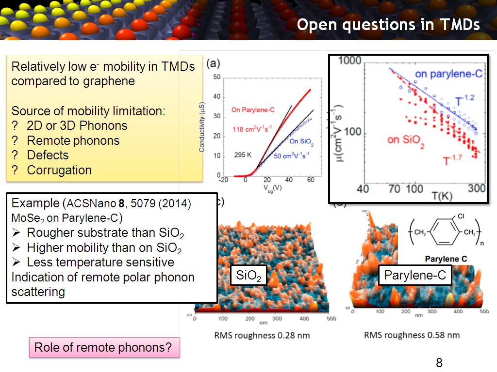 8. Open questions in TMDs
395.92926259592929
00:00/00:00
8. Open questions in TMDs
395.92926259592929
00:00/00:00 -
 9. Open questions in TMDs
469.80313646980318
00:00/00:00
9. Open questions in TMDs
469.80313646980318
00:00/00:00 -
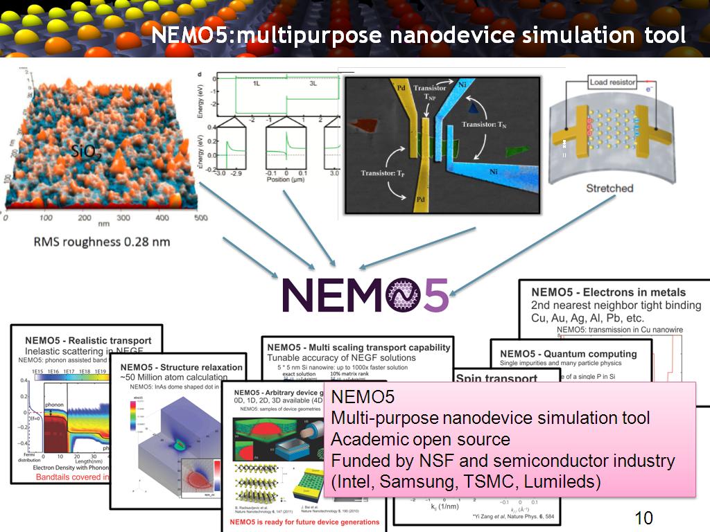 10. NEMO5:multipurpose nanodevice …
550.950950950951
00:00/00:00
10. NEMO5:multipurpose nanodevice …
550.950950950951
00:00/00:00 -
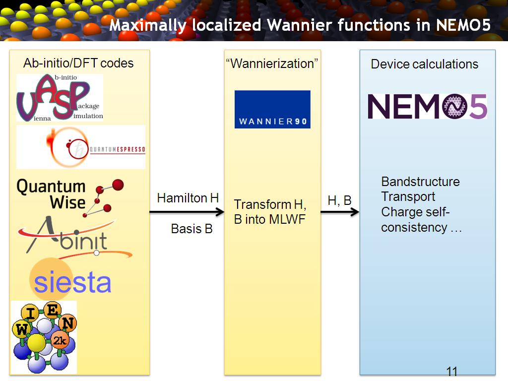 11. Maximally localized Wannier fu…
612.1788455121789
00:00/00:00
11. Maximally localized Wannier fu…
612.1788455121789
00:00/00:00 -
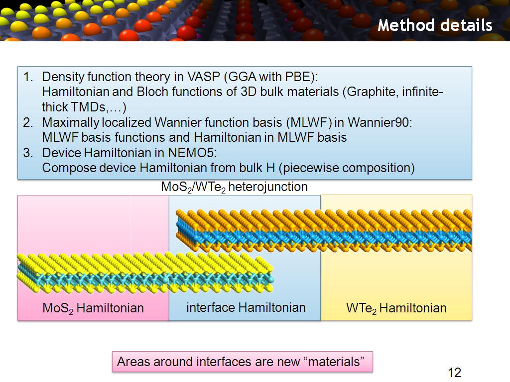 12. Method details
697.96463129796462
00:00/00:00
12. Method details
697.96463129796462
00:00/00:00 -
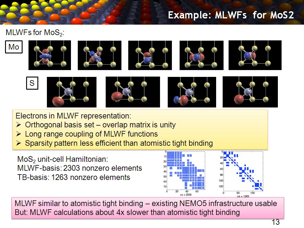 13. Example: MLWFs for MoS2
849.98331664998329
00:00/00:00
13. Example: MLWFs for MoS2
849.98331664998329
00:00/00:00 -
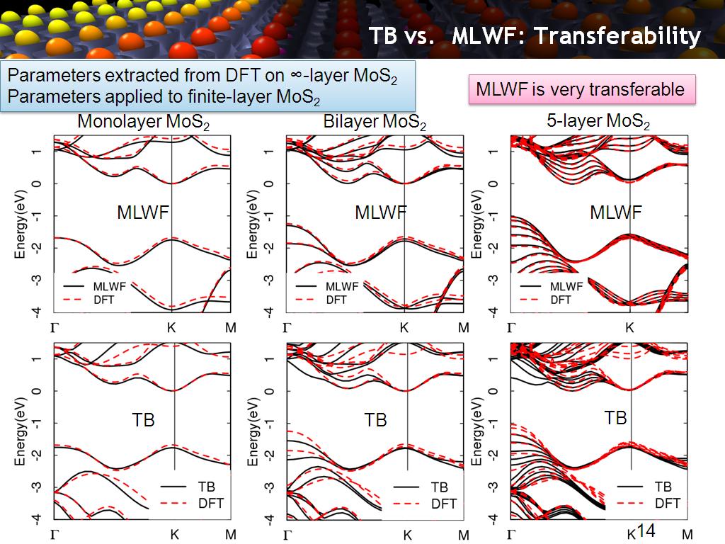
 14. TB vs. MLWF: Transferability
952.585919252586
00:00/00:00
14. TB vs. MLWF: Transferability
952.585919252586
00:00/00:00 -
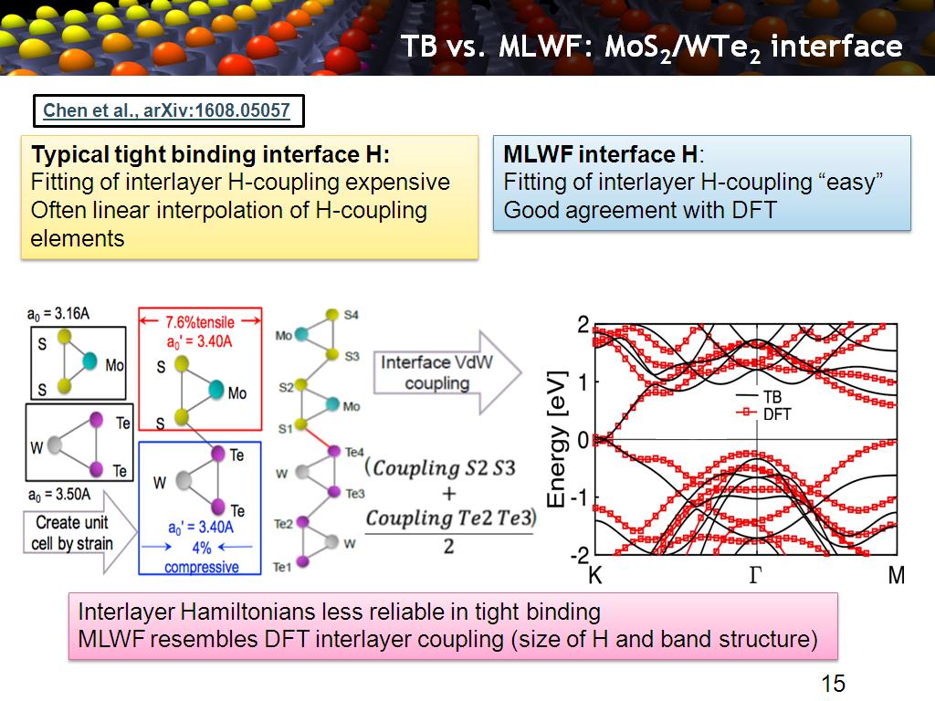 15. TB vs. MLWF: MoS2/WTe2 interfa…
1077.0770770770771
00:00/00:00
15. TB vs. MLWF: MoS2/WTe2 interfa…
1077.0770770770771
00:00/00:00 -
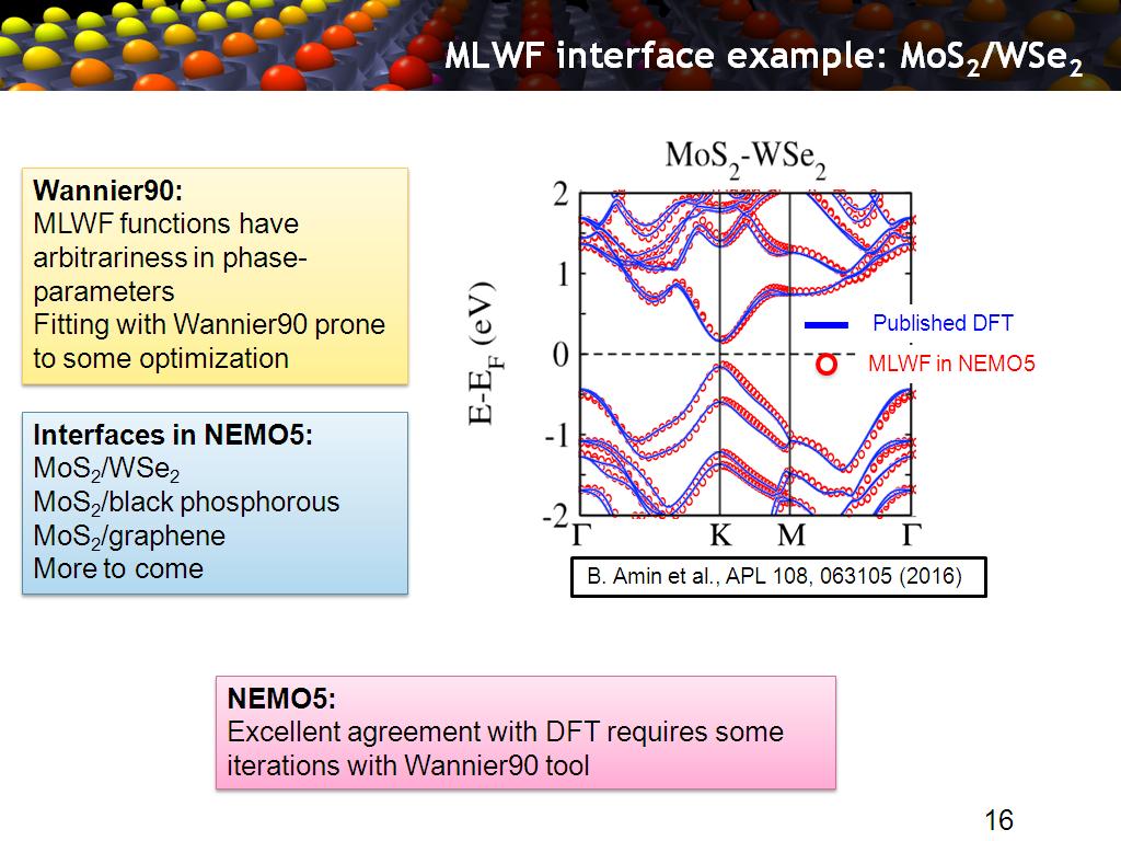 16. MLWF interface example: MoS2/W…
1143.5101768435102
00:00/00:00
16. MLWF interface example: MoS2/W…
1143.5101768435102
00:00/00:00 -
 17. Bandstructure and wave functio…
1181.8485151818486
00:00/00:00
17. Bandstructure and wave functio…
1181.8485151818486
00:00/00:00 -
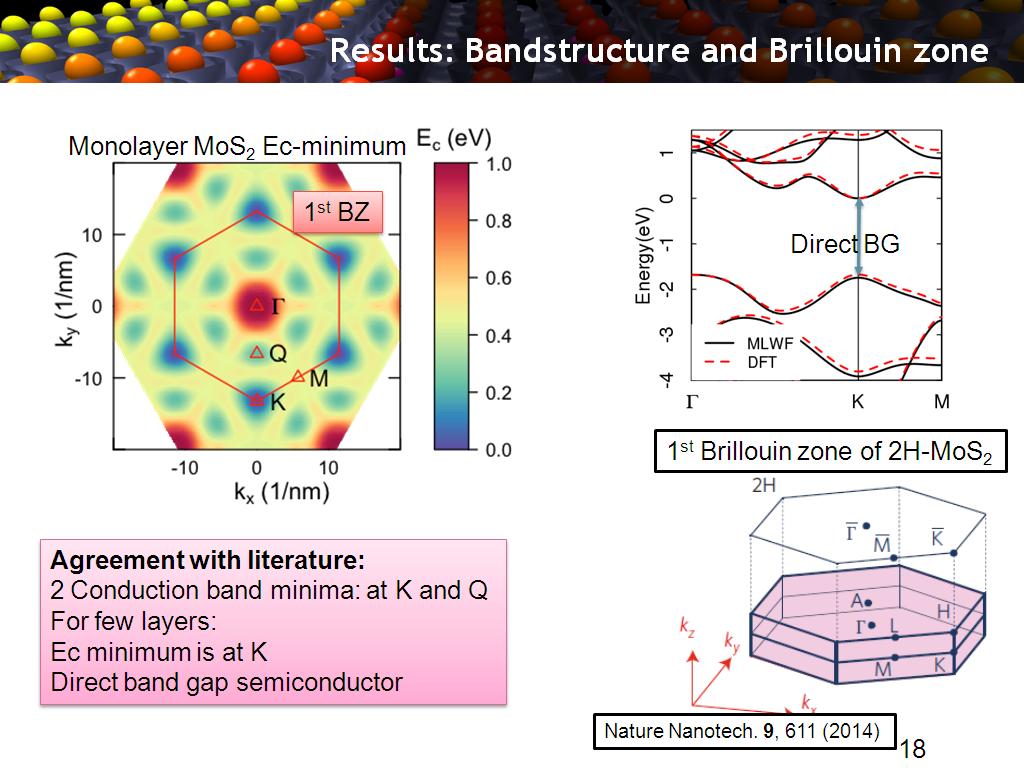
 18. Results: Bandstructure and Bri…
1188.8221554888221
00:00/00:00
18. Results: Bandstructure and Bri…
1188.8221554888221
00:00/00:00 -
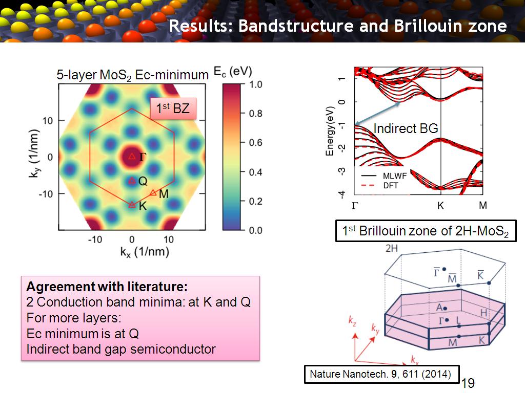
 19. Results: Bandstructure and Bri…
1257.0904237570906
00:00/00:00
19. Results: Bandstructure and Bri…
1257.0904237570906
00:00/00:00 -
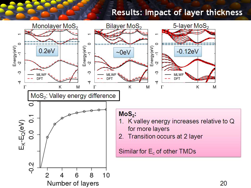 20. Results: Impact of layer thick…
1288.6553219886553
00:00/00:00
20. Results: Impact of layer thick…
1288.6553219886553
00:00/00:00 -
 21. Results: Conduction band wave …
1311.0777444110779
00:00/00:00
21. Results: Conduction band wave …
1311.0777444110779
00:00/00:00 -
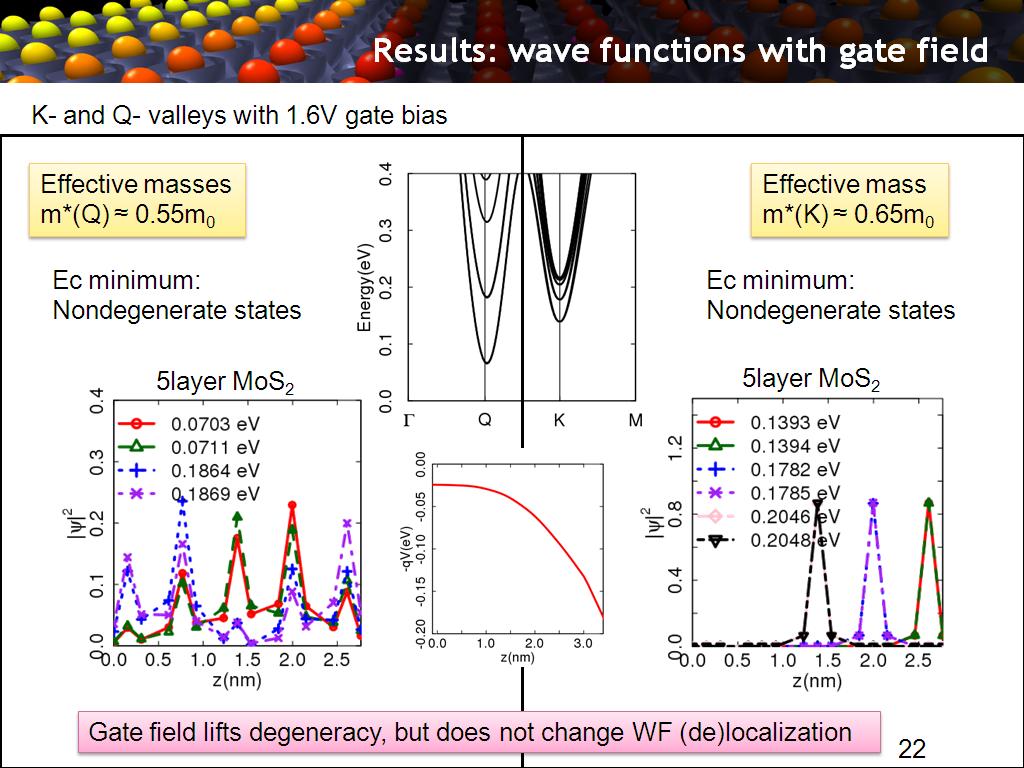 22. Results: wave functions with g…
1339.0056723390057
00:00/00:00
22. Results: wave functions with g…
1339.0056723390057
00:00/00:00 -
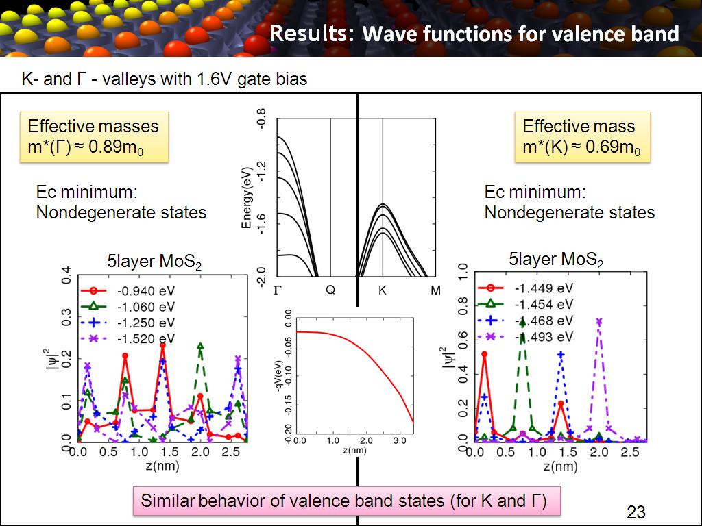 23. Results: Wave functions for va…
1361.0610610610611
00:00/00:00
23. Results: Wave functions for va…
1361.0610610610611
00:00/00:00 -
 24. Device results
1402.4691358024693
00:00/00:00
24. Device results
1402.4691358024693
00:00/00:00 -
 25. Experiment: open question
1404.2042042042042
00:00/00:00
25. Experiment: open question
1404.2042042042042
00:00/00:00 -
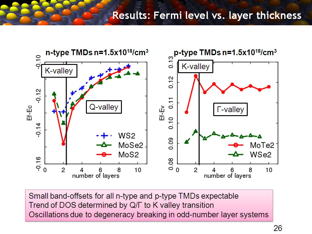 26. Results: Fermi level vs. layer…
1442.9095762429097
00:00/00:00
26. Results: Fermi level vs. layer…
1442.9095762429097
00:00/00:00 -
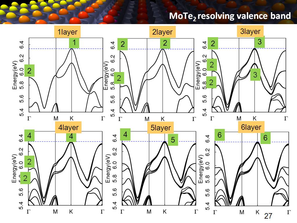 27. MoTe2 resolving valence band
1514.4477811144479
00:00/00:00
27. MoTe2 resolving valence band
1514.4477811144479
00:00/00:00 -
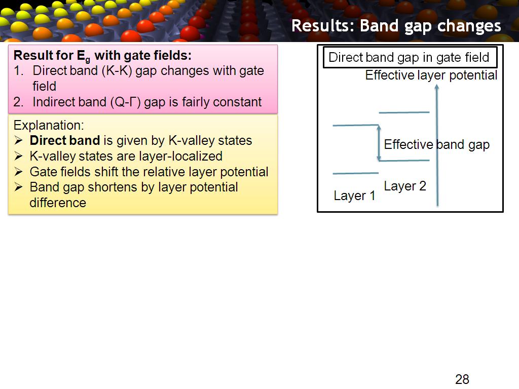
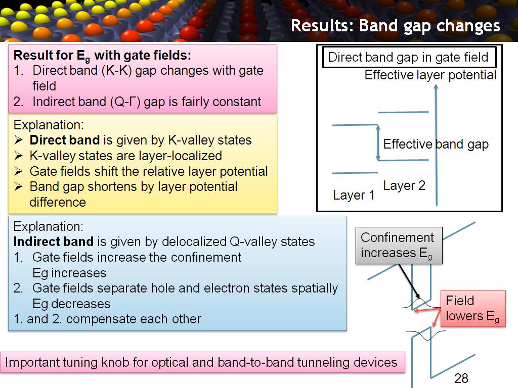 28. Results: Band gap changes
1632.4991658324993
00:00/00:00
28. Results: Band gap changes
1632.4991658324993
00:00/00:00 -
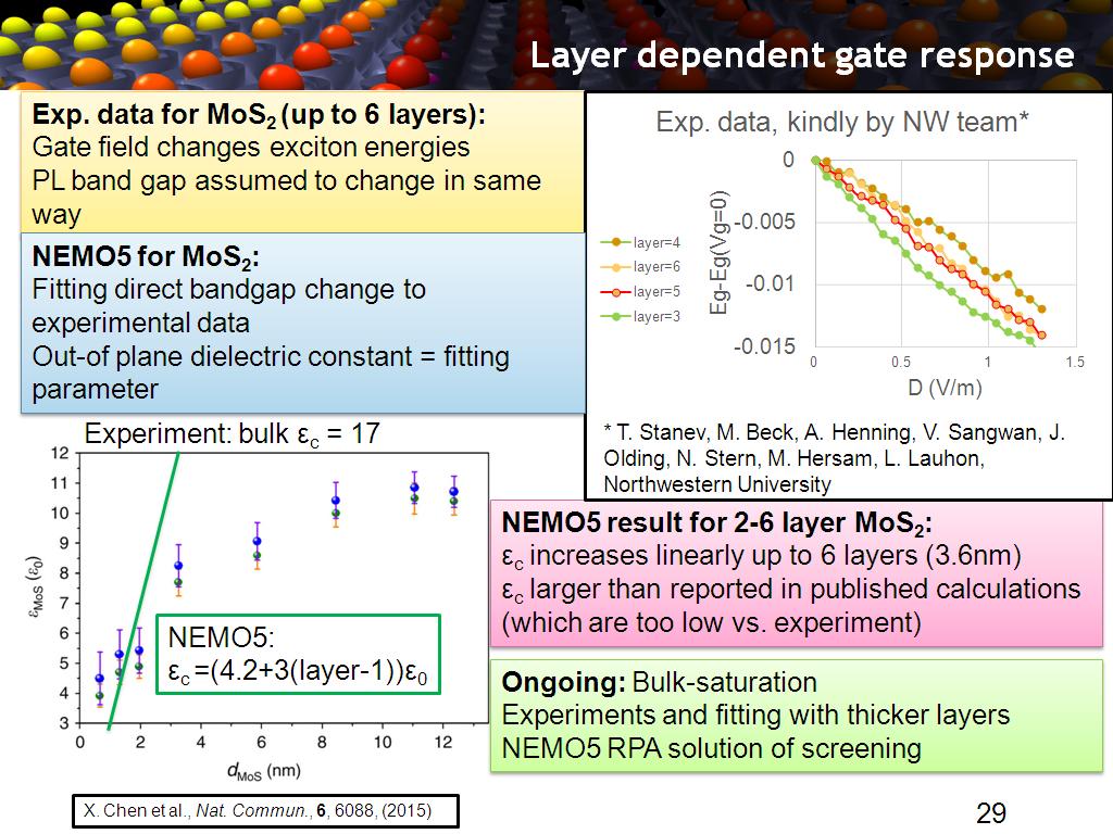 29. Layer dependent gate response
2229.92992992993
00:00/00:00
29. Layer dependent gate response
2229.92992992993
00:00/00:00 -
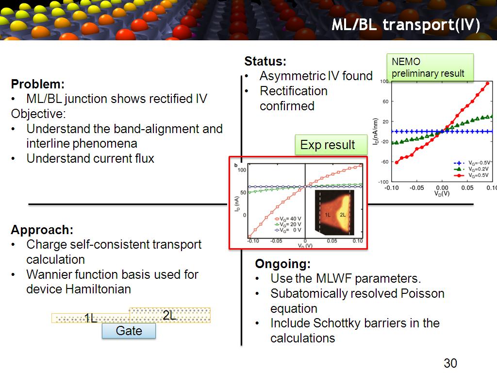 30. ML/BL transport(IV)
2389.456122789456
00:00/00:00
30. ML/BL transport(IV)
2389.456122789456
00:00/00:00 -
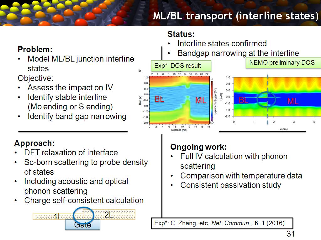 31. ML/BL transport (interline sta…
2432.8661995328662
00:00/00:00
31. ML/BL transport (interline sta…
2432.8661995328662
00:00/00:00 -
 32. Ongoing model development
2532.3656990323657
00:00/00:00
32. Ongoing model development
2532.3656990323657
00:00/00:00 -
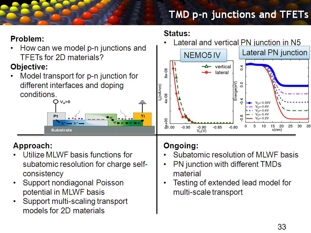 33. TMD p-n junctions and TFETs
2536.3697030363696
00:00/00:00
33. TMD p-n junctions and TFETs
2536.3697030363696
00:00/00:00 -
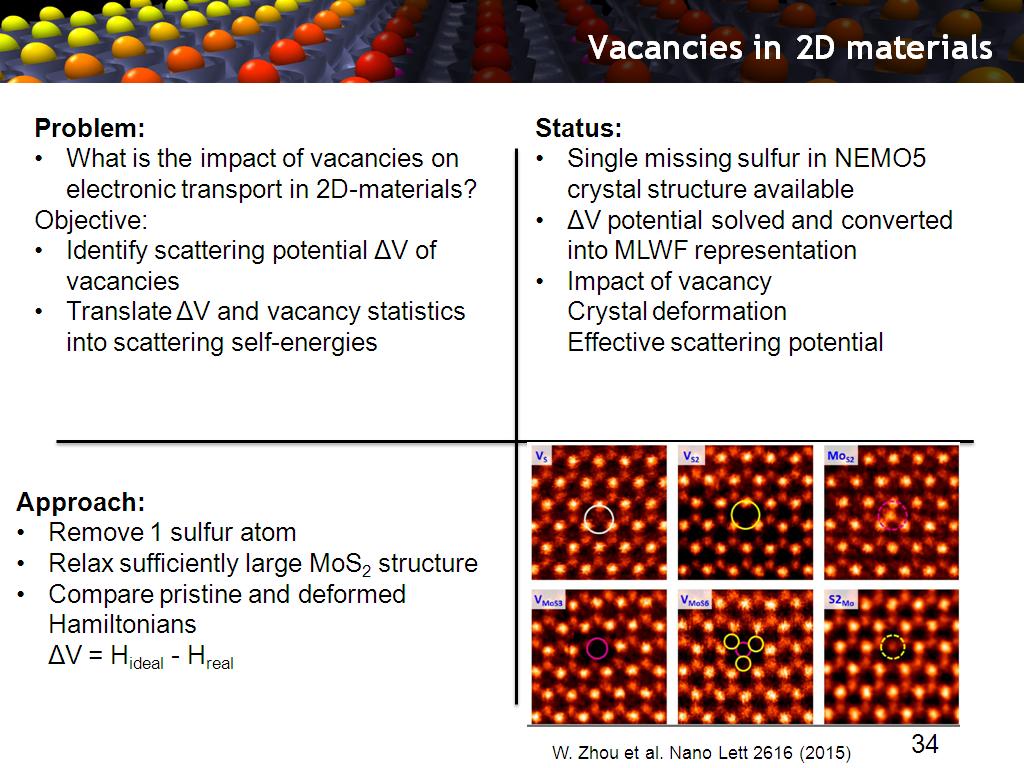 34. Vacancies in 2D materials
2623.1231231231232
00:00/00:00
34. Vacancies in 2D materials
2623.1231231231232
00:00/00:00 -
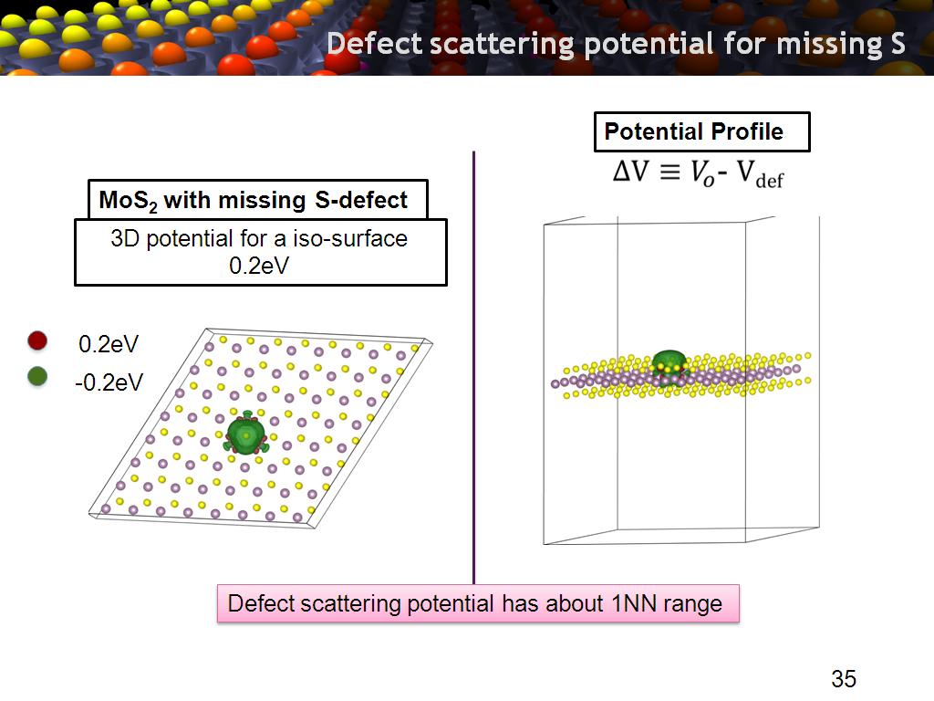 35. Defect scattering potential fo…
2697.4974974974975
00:00/00:00
35. Defect scattering potential fo…
2697.4974974974975
00:00/00:00 -
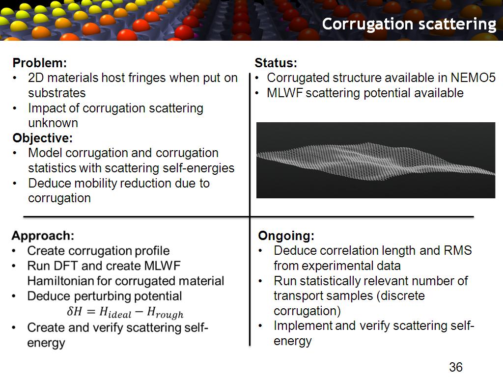 36. Corrugation scattering
2727.0270270270271
00:00/00:00
36. Corrugation scattering
2727.0270270270271
00:00/00:00 -
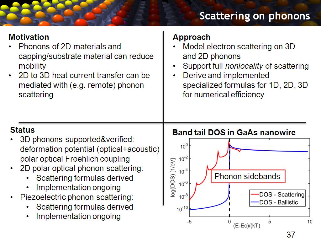 37. Scattering on phonons
2883.6503169836506
00:00/00:00
37. Scattering on phonons
2883.6503169836506
00:00/00:00 -
 38. Efficient algorithm for nonloc…
2969.5695695695695
00:00/00:00
38. Efficient algorithm for nonloc…
2969.5695695695695
00:00/00:00 -
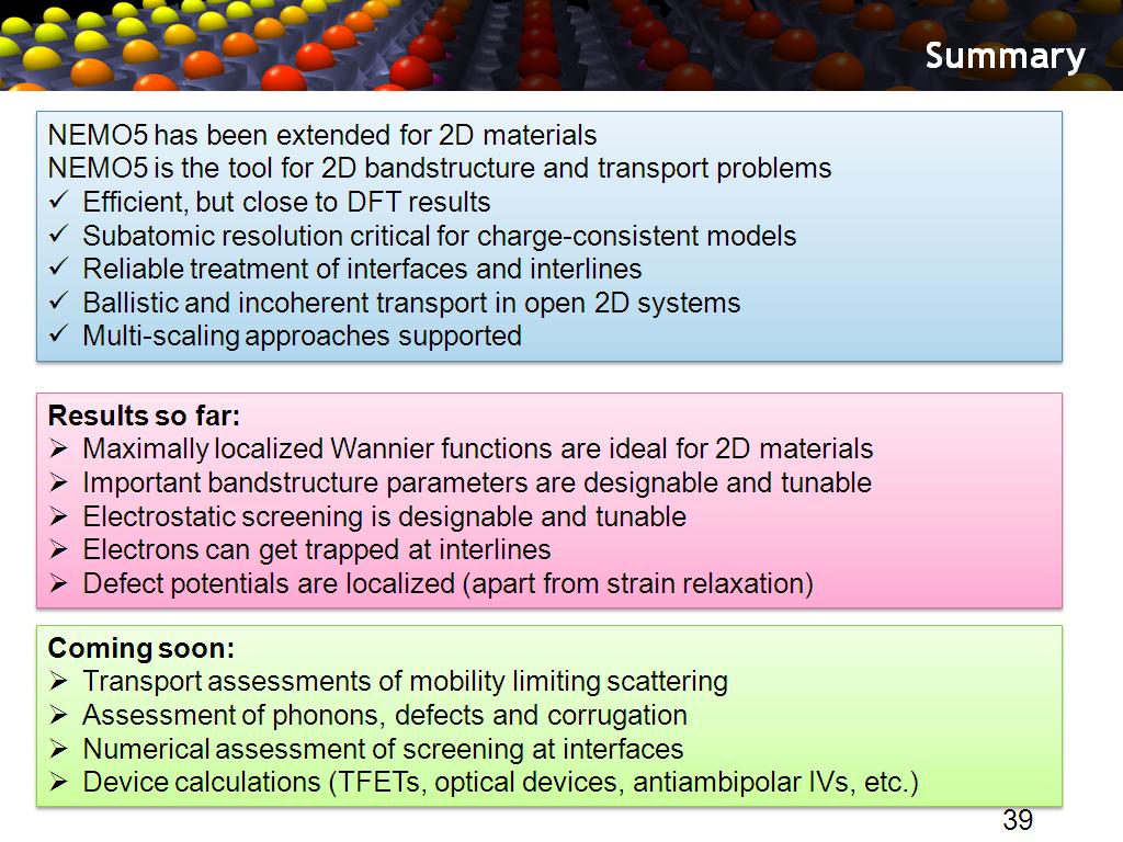 39. Summary
3064.3643643643645
00:00/00:00
39. Summary
3064.3643643643645
00:00/00:00 -
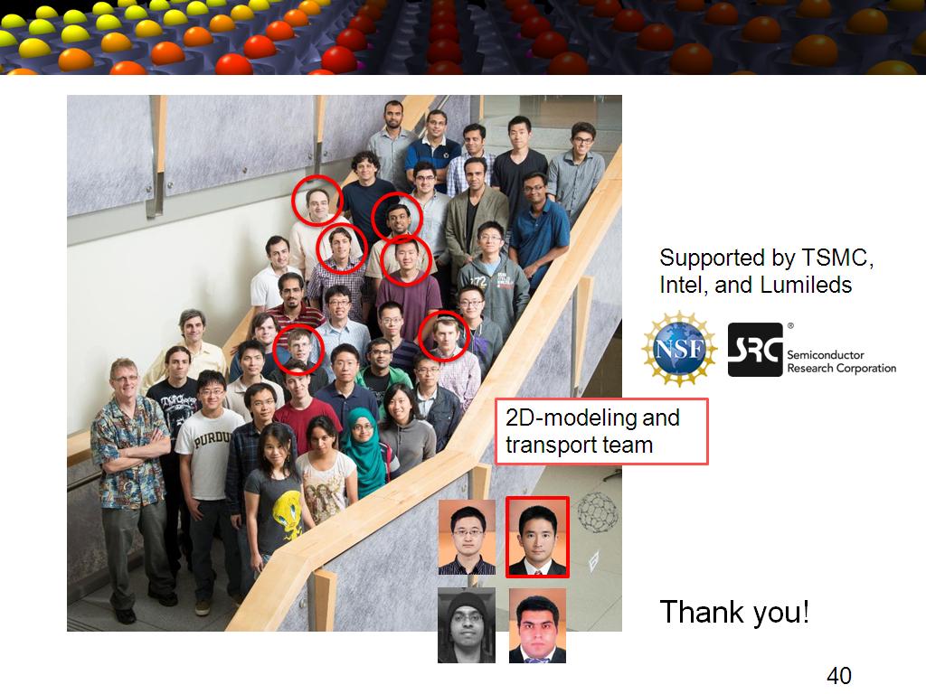 40. Thank you!
3205.7057057057059
00:00/00:00
40. Thank you!
3205.7057057057059
00:00/00:00