Upcoming Electron Microscopy Capabilities at Purdue University: Structural, Chemical and Electronic Characterization at the Atomic Level of Complex Nano-materials
Category
Published on
Abstract
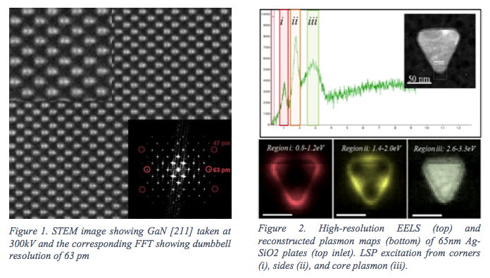
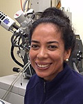
The acquisition of new state of the art TEM – Themis Z – at Birck Nanotechnology Center will enable users across a wide range of research areas to acquire a higher understanding of nano‐materials at the atomic level. Researchers at Birck will be able to gain fundamental understanding of the materials’ physical and chemical properties and a proper correlation between these properties and morphology at the nanoscale. The Thermo Fisher Themis Z TEM is equipped with a probe and image aberration correctors to assure sub‐angstrom resolution in STEM and TEM across the entire acceleration voltage range of 60 to 300 kV, the microscope delivers a STEM and TEM resolution down to 60 pm at 300kV and 140 pm and 180 pm at 60kV (Figure 1). The Themis Z TEM is also is equipped with a monochromator and Electron Energy Loss Spectrometer (EELS) to EELS spectrometer that assures an energy resolution of 80meV at 60kV to suit all EELS applications. This kind of energy resolution will enable researchers at Birck to study plasmonic structures or any other material with emissions in the visible range of the electromagnetic spectrum (Figure 2). Additionally, the Themis Z TEM has a Super X EDX detector that delivers high signal to noise ratio for optimum EDX results. During my talk, I will be presenting different applications for each of these new capabilities, which are relevant to nanomaterials developed and studied in our institution.
Bio
 Rosa has over 8 years of experience on aberration corrected transmission electron microscopes (TEM) and environmental TEM (E‐TEM). She graduated from Arizona State University in 2010 with a PhD in Materials Science and Engineer. She later went to work as a postdoc at Brookhaven National Laboratory under the supervision of former Purdue alumni Eric Stach. Her work involved the design and implementation of in‐situ experiments to study catalytic systems as well as growth of 1D nanostructures using an image‐corrected E‐TEM and a probe‐corrected STEM. Subsequently, she moved to Okinawa Institute Science and Technology as a staff scientist to work with their aberration corrected and monochromated E‐STEM. Her work focused mainly on using advanced analytical techniques to study modifications of nanoparticle systems with applications in biomedicine. Rosa has been at Birck for 3 years assisting Birck users with understanding the structural and chemical characteristics of their nanomaterials ranging from optoelectronics, catalysis, and metallic alloys to biomaterials. She is also the microscopist for the Microsoft Station Q Purdue Project under the direction of Prof. Michael Manfra. Rosa’s main research interest focuses on understanding superconducting‐ semiconductor interface with high resolution TEM and STEM, understanding plasmonic and biomaterials with high resolution EELS, and studying the modification of materials in‐situ under changing temperature and gas conditions.
Sponsored by
Cite this work
Researchers should cite this work as follows:
Time
Location
Room 1001, Birck Nanotechnology Center, Purdue University, West Lafayette, IN