09 Demonstration of Vertical GaN PN Diode with Step-etched Triple zone JTE
Category
Published on
Abstract
Day 4, Session 2.2
Introduction: Recently, significant research of vertical GaN power devices using GaN layers grown on bulk GaN substrate that have lower dislocation density (>106 cm-2) have been carried out to achieve improved reliability, yield, and reverse characteristics. It is essential for power devices to achieve high edge termination efficiency using the proper edge termination technique. Power devices without edge termination show considerably lower breakdown voltage than the ideal case due to electric field crowding effect at the junction periphery [1]. Since patterned p-type doping for GaN is very challenging [2] for guard ring [3] and PN JTE [4], various studies for edge termination techniques are needed to obtain high edge termination efficiency for vertical GaN power devices with higher breakdown (BV) capability (>10-20 kV). Here, based on simulation, we fabricated and demonstrated vertical GaN PN diode with step-etched triple zone JTE (STJTE) on bulk substrate.
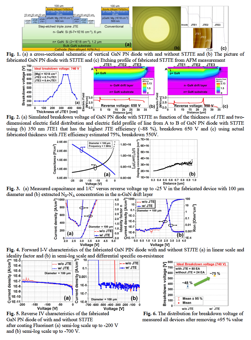
Growth, Design, and Fabrication: Fig. 1(a) shows a cross-sectional schematic of vertical GaN PN diode with and without STJTE. All layers for this study were grown by MOCVD. The epitaxial layers consist of a 20 nm p+ GaN (Mg: 1019 cm-3) contact layer, a 500 nm p-GaN layer (Mg: 1018 cm-3), a 6 μm n-GaN drift layer (Si: 5-6×1016 cm-3), a 1.2 μm n+GaN layer (Si: 2×1018 cm-3) on thick bulk GaN substrate. The Pd/Ni/Au metal stack were deposited on p+GaN layer to form p-GaN ohmic contact, followed by RTA at 400 ◦C for 1 min at N2 ambient. The diameter of electrode is 100 μm. Mesa isolation of 1 μm was carried out by ICP-RIE. The specific contact resistance of pGaN is ~ 1 mΩ·cm2 extracted from TLM. A non-alloyed Al/Ni/Au metal stack was deposited on the bottom of GaN substrate. Each JTE regions were etched by ICP-RIE with different etching time. Fig. 1(b) shows the picture of the fabricated GaN PN diode with STJTE. The etching profile of fabricated JTE regions was measured by AFM as shown in Fig. 1(c). To achieve the optimal thickness of STJTE for higher JTE termination efficiency, we performed 2D simulation. BV was defined as the applied voltage when peak electric field exceeds 3 MV/cm. The total length of JTE region was 30 μm which was selected to be five times the thickness of the drift layer [5]. The ratio of each JTE thickness was fixed as JTE1:JTE2:JTE3=1:0.7:0.4. Fig. 2(a) shows the simulated BV of GaN PN diode with STJTE as a function of the thickness of JTE1. Ideal BV was 740 V. JTE1 of 350 nm exhibited the highest JTE efficiency which is 88 % (650 V) as shown in Fig. 2(a).
Results: The net doping concentration (ND-NA) in the n-GaN drift layer can be extracted from C-V measurement as shown in Fig. 3, and were estimated to be (2~3)×1016 cm-3. Fig. 4 shows the forward I-V characteristics of the fabricated GaN PN diode with and without STJTE at room temperature. The fabricated devices showed that the turn-on voltage (at 100 A/cm2) was 3.1 V, the lowest ideality factor was 1.3, and On-off ratio was ~1011. Based on 2D simulation for maximum current spreading, the bottom diameter of with JTE and without JTE considering maximum current spreading was 111 μm and 108 μm, respectively. Thus, differential specific on- resistance using each diameter at 1 kA/cm2 with and without STJTE was identical which is ~1.3 mΩ·cm2. Fig. 5 shows reverse I-V characteristics. Reverse leakage current at -200 V of with and without STJTE were 80 nA/cm2 and 186 nA/cm2, respectively. The destructive BV with and without STJTE were 550 V and 330 V, respectively. Fig. 6 shows the distribution for BV of all measured devices showing a destructive failure. The average BV of without STJTE was 360 V, which is ~48 % JTE efficiency, and that of with STJTE was 550 V which is ~75 % JTE efficiency. While the demonstrated BV does show the efficacy of this method for edge termination, the experimental value is still lower than the simulated value (88%) discussed earlier. The actual etch depth for the device was 105 nm, compared to the design value of 130~150 nm. The device with the actual experimentally achieved JTE etch depth was simulated. The results are shown in Figure 2(c). The simulations show a higher peak field at the edge of JTE3 region, and an expected BV (550 V simulated) which matches the experimentally achieved value.
Conclusion: We have demonstrated significantly improved BV of vertical GaN PN diode with STJTE without any degradation of forward characteristics. This is the first demonstration of a step-etched multiple zone edge termination for III-Nitride technology.
Credits
The information, data, or work presented herein was funded in part by the Advanced Research Projects Agency-Energy (ARPA-E), U.S. Department of Energy, under Award Number DE-AR0001036.
Sponsored by
References
- V. A. K. Temple et al, IEEE Trans. Electron Devices, 22, 910 (1975);
- M. J. Tadjer, et al, ECS J. Solid State Sci. Technol, 5, 124 (2016);
- D. C. Sheridan et al, Solid-State Electron., 44, 1367 (2000);
- H Miyake et al, IEEE Electron Device Lett., 33, 1598 (2012);
- D. C. Sheridan et al, Solid-State Electron., 45, 1659 (2001)
Cite this work
Researchers should cite this work as follows:
Time
Location
DRC 2020 Virtual Conference