Objective of Lesson: To learn how to depict a crystal on a two-dimensional surface
Reading Assignment: 2.2.1
Discussion Questions:
1. How much paper would it take to show a silicon crystal at room temperature with a representative number of broken bonds?
2. How are broken bonds in the bonding model depicted in the energy band model?
Homework:
1. Draw a bonding model representation of GaAs.
2. Draw a bonding model representation of silicon with a missing silicon atom.
3. Draw a bonding model representation of silicon with a silicon atom replaced by a carbon atom.
What do you need to know for the exam?
1. You need to be able to draw a bonding model representation of anything—most of which we have not yet covered. These things will be described later such as in
the dopants section.
Summary
The bonding model is a very important visualization aid used in the analysis of semiconductor devices. It is the visualization of the bonding that takes place between the atoms inside a semiconductor crystal, or, to put it simply, it is a two-dimensional representation of the semiconductor crystal.
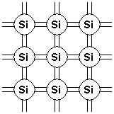 {{{
Figure 1}}}
{{{
Figure 1}}}
The Bonding Model
Figure 1 shows a two-dimensional representation of a silicon crystal. We have to show it in two dimensions as that is what paper and chalkboards allow. The circles are silicon atoms and the lines represent valence bonds formed by valence electrons. Note that each atom has eight lines emanating from it, representing the eight shared electrons that hold the crystal together.
The bonding model is mostly used to give a basic idea of what the individual electrons are doing in the semiconductor. It takes advantage of the fact that the structure of a polycrystalline or crystalline material is uniform and virtually identical throughout. It demonstrates the actions of an electron with only a few samples, very much like looking at it through a microscope.
When an electron gains enough energy, either through thermal vibrations or some other mechanism, it breaks free from its native atom and can move around, thus transporting its charge within the crystal lattice. This free electron is shown as a broken bond and/or a negative charge leaving the atom, and this identifies it as a carrier of charge.
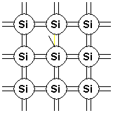 {{{
Figure 2. Bonding model diagram showing bond broken by thermal energy.}}}
{{{
Figure 2. Bonding model diagram showing bond broken by thermal energy.}}}
The broken bond that creates the free electron leaves behind a positively charged vacancy that behaves like a new entity that we call the hole. A hole can move through the lattice as an electron does and it is also a carrier—we treat it like a positively charged particle.
A point defect is when an atom is missing or an impurity is present in the crystal structure, and the bonding model can illustrate either of these.
The bonding model qualitatively describes the semiconductor lattice well, but it is impractical for quantitative analysis, because the analysis can get more complicated mathematically. The bonding model is rarely used, but it helps us visualize what is going on inside the semiconductor. Therefore, being able to understand the bonding model, drawing it and interpreting it, is one of the first steps needed to understand future concepts.
Bond: A mechanism by means of which atoms, ions or groups of atoms are held together in a molecule or crystal.
Model: A tentative description of a system or theory that accounts for all of its known properties.