Welcome to ANTSY – Assembly for Nano Technology SurveY courses!
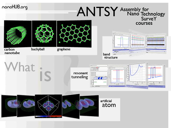
This ANTSY support wiki page gathers educational materials that are related to the ANTSY tool. ANTSY assembles several nanoHUB tools that we think can be useful for entry-level courses that aim to provide insights into nanotechnology structures like carbon nanotubes, graphene, quantum dots, and superlattices. We have gathered exercises, assignments, and quizzes that have been contributed to nanoHUB by several authors.
Anyone is invited to contribute new resources to nanoHUB as an open-access platform. We would welcome your exercises, homework assignments or quizzes. Some of the material available below is using flash technology that is becoming outdated. We are working on updating the material.
Each of the individual tools has
- a Q/A forum, where you can post public questions and find answers. This forum is supported by the volunteer tool contributors.
- a wishlist, where you can request feature updates or improvements to the community
- a “help” link on the top right of the page, where you can file a support ticket if something goes wrong on the tools or that tool pages.
This wiki page allows you to leave comments. Please be explicit and provide constructive feedback.
We are funded by the US National Science Foundation (NSF) since 2002 and provide a service that is free to you. We gather systematic evidence of impact on education and research. Yet, notable quotes from community members help to put “a face” on impact stories. We hope you find ANTSY and nanoHUB useful and we invite you to leave your success story to share.
All simulation tools and feedback mechanisms require you to login and to authenticate yourself via various social networks, your institutional account, or via a new nanoHUB login.
Structures: Bucky Balls, Carbon Nanotubes, Graphene, Crystal Structures, and Lattices
Crystal Viewer

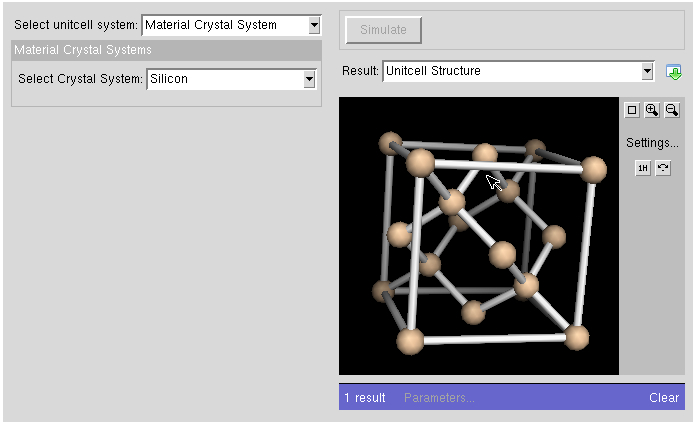
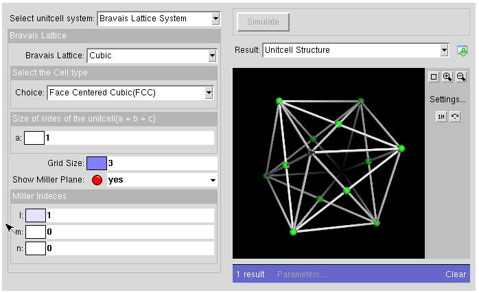
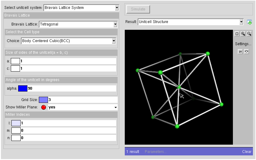
The Crystal Viewer in ANTSY enables the interactive visualization different Bravais lattices, crystal planes, and materials (diamond, silicon, indium arsenide, gallium arsenide, graphene, and buckyball). We are in the process of creating a new, more interactive version of Crystal Viewer, to be released around the 20th of August.
For Crystal Viewer there are several additional resources:
- First-Time User Guide (which needs some updating from the prior tool version look)
- A homework assignment in MS Word and Adobe PDF format.
- An Exercise on Crystal Lattices
Carbon Nanotubes and Graphene Sheets
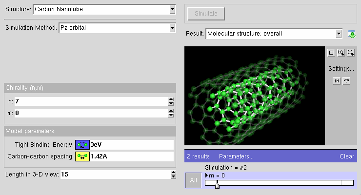
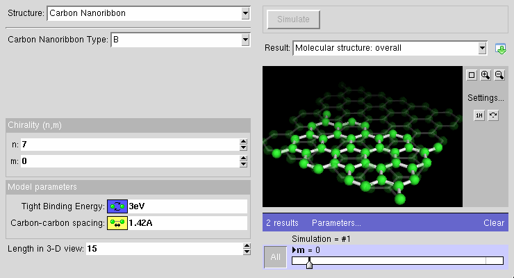
Carbon nanotubes and graphene ribbons made of the single element carbon have attracted significant interest in the nanotechnology research community. The CNTbands tool in ANTSY allows students to visualize the geometries of materials and study their electronic structure.
Exercises :
- exercise 1, atomistic structure
- exercise 2, armchair CNTs
- exercise 3, zig-zag CNTs
- exercise 4, diameter dependence CNTs
Closed Systems – Electronic States
Quantum Dot Lab
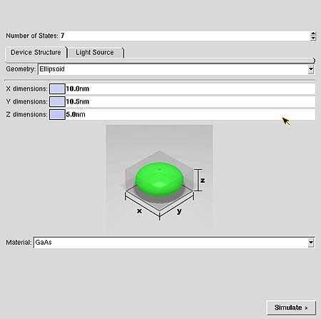

Individual quantum dots can be created from two-dimensional electron or hole gases present in remotely doped quantum wells or semiconductor heterostructures. The sample surface is coated with a thin layer of resist. A lateral pattern is then defined in the resist by electron beam lithography. This pattern can be transferred to the electron or hole gas by etching or by depositing metal electrodes (lift-off process) that allow the application of external voltages between the electron gas and the electrodes. Such quantum dots are mainly of interest for experiments and applications involving electron or hole transport, i.e., an electrical current. The energy spectrum of a quantum dot can be engineered by controlling the geometrical size, shape, and strength of the confinement potential. Also, in contrast to atoms, it is relatively easy to connect quantum dots to conducting leads using tunnel barriers, which allows the application of the techniques of tunneling spectroscopy for their investigation. Confinement in quantum dots can also arise from electrostatic potentials (generated by external electrodes, doping, strain, or impurities).
Quantum Dot Lab in ANTSY computes the eigenstates of a particle in a box of various shapes, including domes and pyramids.
Lectures and Exercises:
- A lecture in flash and pdf starts from particle-wave duality and explores the concepts of quantum dots.
- Introduction to Quantum Dot Lab is a lecture with exercises in flash and pdf form.
Exercises:
Open Systems – Electron Transport
Piecewise Constant Potential Tool
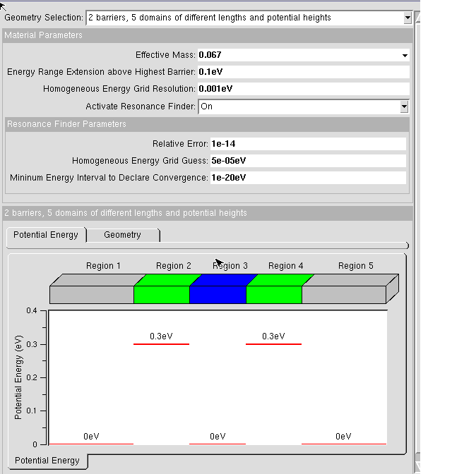

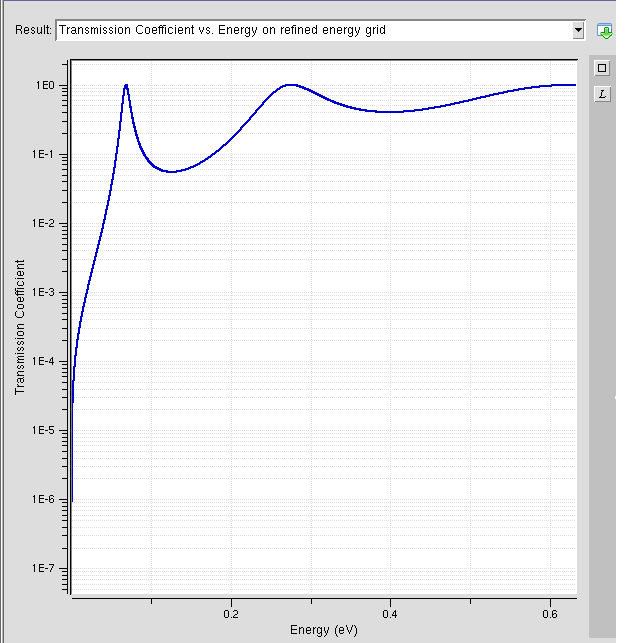
The Piece-Wise Constant Potential Tool in ANTSY allows users to calculate the transmission and the reflection coefficient of arbitrary five, seven, nine, eleven and 2n-segment piecewise constant potential energy profile. For the case of a multi-well structure, it also calculates the quasi-bound states. Thus the Piecewise Constant Potential Tool can be used as a simple demonstration tool for the formation of energy bands. Other uses include: 1) in the case of stationary perturbation theory, as an exercise to test the validity of the first-order and the second-order correction to the ground state energy of the system due to small perturbations of the confining potential, and 2) as a test of the validity of the Wentzel–Kramers–Brillouin (WKB) approximation for triangular potential barriers.
Exercises:
- Quantum-Mechanical Reflections: an Exercise
- Double-Barrier Case: An Exercise
- From 1 well to 2 wells to 5 wells to periodic potentials: an Exercise
- Energy Bands as a Function of the Geometry of the n-Well Potential: an Exercise
- Cosine Bands: an Exercise for PCPBT
- Quantum-Mechanical Reflections in Nanodevices: an Exercise
- Tunneling Through Triangular Barrier: an Exercise for PCPBT
- Stationary Perturbation Theory: an Exercise for PCPBT
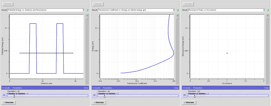
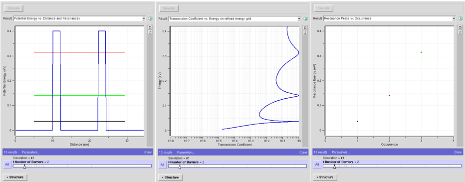
Resonant Tunneling Diode Lab
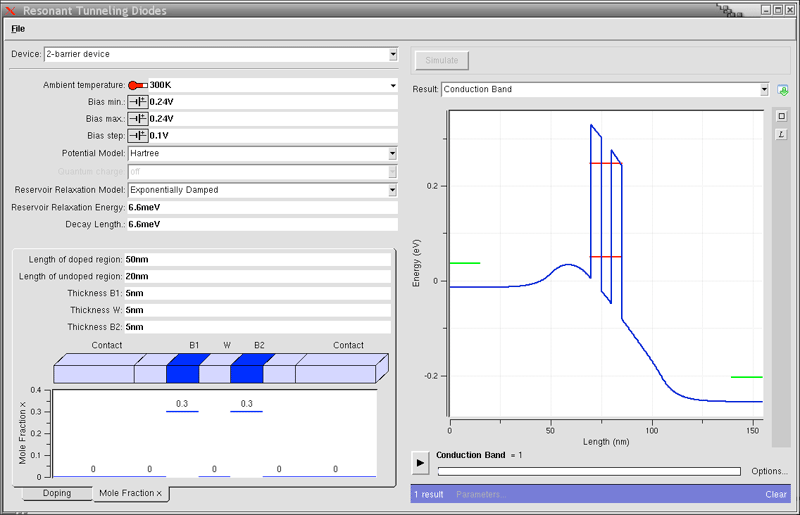
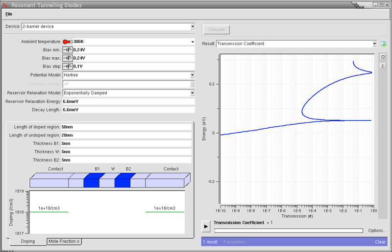
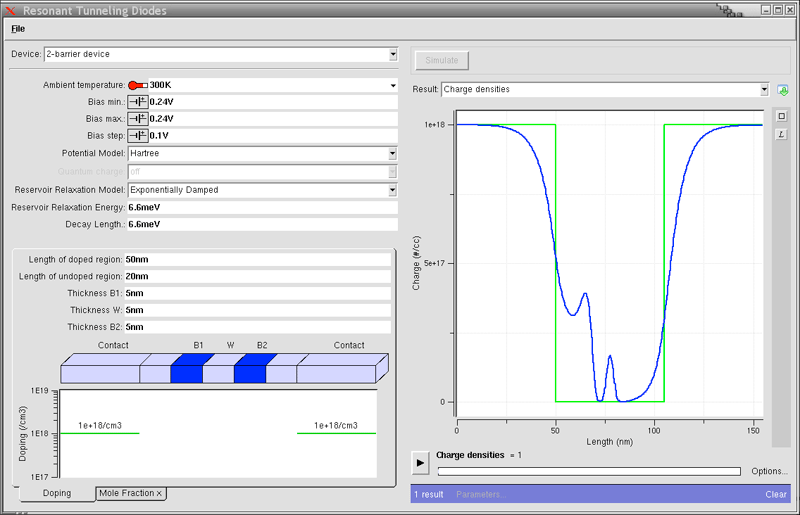
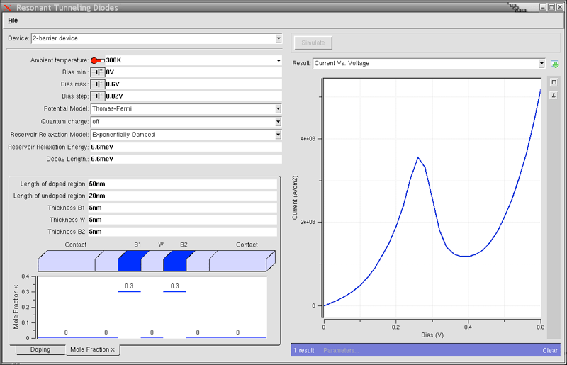
A barrier placed in the path of electrons will block their flow. If the barrier is too thin, however, the electrons can tunnel through it because of quantum mechanical effects. Furthermore, if two or more thin barriers are placed in close proximity, electrons will bounce between the barriers and, at certain resonant energies, begin to flow through the barriers.
The Resonant Tunneling Diode Lab in ANTSY allows users to experiment with this quantum mechanical phenomenon by controlling the number of barriers and their material properties and then simulate current as a function of bias.
Exercises:
About ANTSY Constituent Tools
The Assembly of Basic Applications for Coordinated Understanding of Semiconductors (ANTSY) has been put together from individual tools to provide educators and students with a one-stop-shop in semiconductor education. It therefore benefits tremendously from the hard work that the contributors of the individual tool builders have put into their tools.
As a matter of credit and ranking, simulation runs that are performed in the ANTSY tool are credited to the individual tools. We count the number of usages of the individual tools in the ANTSY tool set to measure the impact of ANTSY and to gather data we can use to improve the tool.
In the description above we do not refer to the individual tools since we want to guide the users to the composite ANTSY tool. We cite the individual tools here explicitly so they are being given the appropriate credit and on their respective tool pages, on which there are links to ANTSY.
Crystal Viewer Tool, Piece-Wise Constant Potential Barriers Tool, Resonant Tunneling Diode Simulation with NEGF, Quantum Dot Lab, and CNTbands.
Additional Reading and Tools
Tool-Powered Curricula
ANTSY is part of the series of Tool-Powered Curricula
Educators
Use the Tool-Powered Curriculum to augment existing courses and enhance the student learning. Use turn-key simulation tools to teach concepts, design, and optimization without reading big manuals and installing software. Use it in your class room or for student assignments such as homework’s or projects. ABACUS and AQME are tools which pull together many different nanoHUB tools into a single interface and are augmented with homework and project assignments. Solutions to homework assignments are available to educators upon request.
“… and more”: Augment your class though interactive lectures from leading researchers providing tool tutorials, nano101 and nano501 lectures. Use community-contributed homework and project assignments in your class. Most lectures are available for interactive online viewing, as pdf downloads, and even podcasts.
Show a student and they will remember; involve them, and they will understand.
Students:
Enjoy using intuitive and user-friendly tools without software installation and reading massive manuals! You will be able to ask “what if?” questions and get answers rapidly to develop intuition and insight. Register for a free nanoHUB account or log into your existing nanoHUB account and begin teaching and learning with the tool powered curriculum.
ABACUS—Assembly of Basic Applications for the Coordinated Understanding of Semiconductors
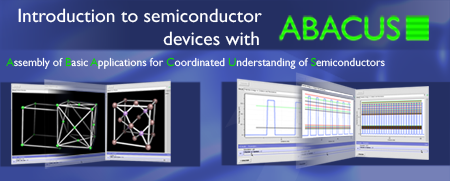
The curriculum entitled Introduction to Semiconductor Devices is powered by the tool ABACUS. The ABACUS powered curriculum is designed to enhance the learning experience of students in existing classes on semiconductor devices in Electrical Engineering curricula. ABACUS is an assembly of different nanoHUB tools that range from crystals, bandstructure, pn junctions, and transistors.
The ABACUS powered curriculum is a curated page that provides easy access to a variety of different homework and project assignments that are relevant for the teaching of semiconductor devices. Educators can request access to homework solutions. Any community members are encouraged to contribute content to the nanoHUB. We encourage you to alert the authors of the curated page to your contribution for possible inclusion.
AQME—Advancing Quantum Mechanics for Engineers
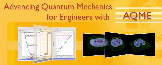
The curriculum entitled Quantum Mechanics for Engineers is powered by the AQME tool which is an assembly of tools we believe are useful in the teaching of introductory quantum mechanical principles in an electrical engineering or physics curriculum. Commercial semiconductor devices have become as small as a few tens of nanometers and understanding basic quantum mechanical principles of quantization, bands, and tunneling are of critical importance.
The AQME powered curriculum is a curated page that provides access to a variety of different homework and project assignments that are relevant for quantum mechanical principles. Educators can request access to homework solutions. Any community members are encouraged to contribute content to the nanoHUB. We encourage you to alert the authors of the curated page to your contribution for possible inclusion.