ECE 606 L20.3: PN Diode - Forward Bias - Non-Linear Regime
ECE 606 L20.3: Forward Bias - Non-Linear Regime

-
 1. Section 20.3 Forward Bias - No…
0
00:00/00:00
1. Section 20.3 Forward Bias - No…
0
00:00/00:00 -
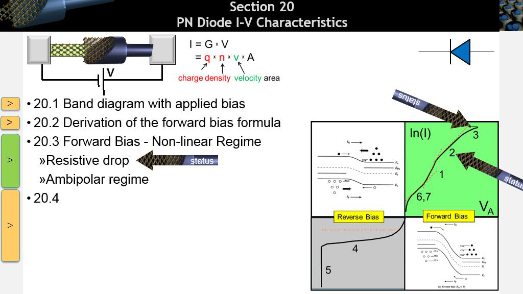 2. Section 20 PN Diode I-V Charac…
20.653987320653989
00:00/00:00
2. Section 20 PN Diode I-V Charac…
20.653987320653989
00:00/00:00 -
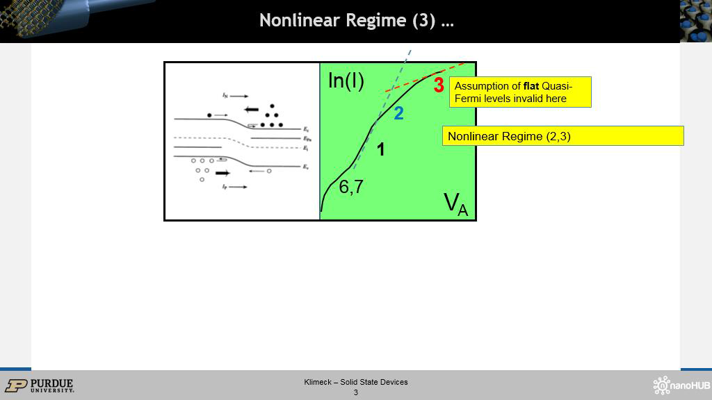
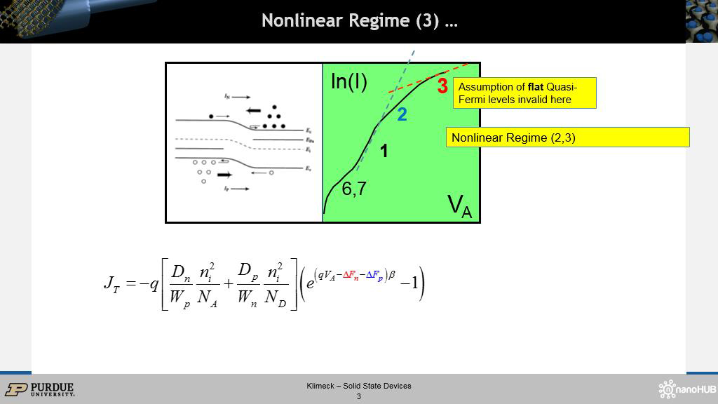
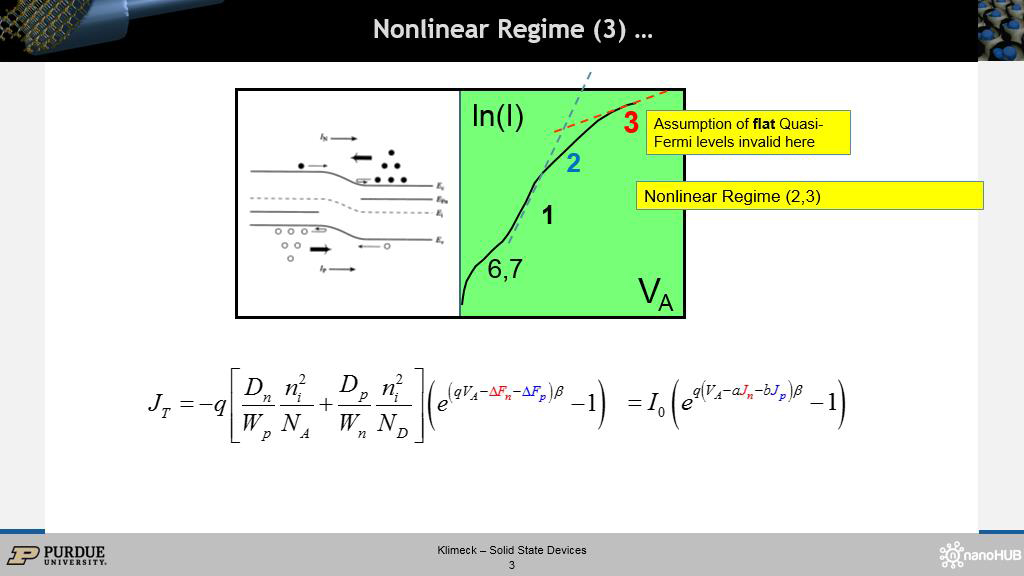
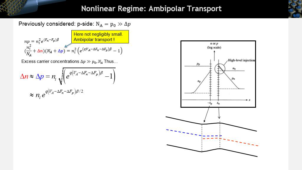
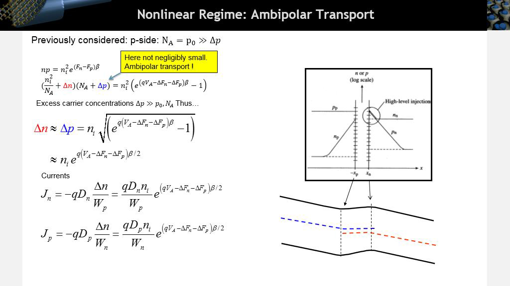
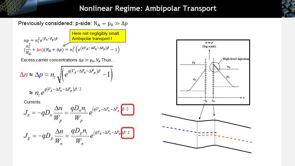
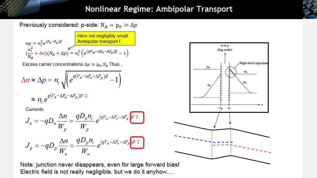
 3. Nonlinear Regime (3) …
34.534534534534536
00:00/00:00
3. Nonlinear Regime (3) …
34.534534534534536
00:00/00:00 -
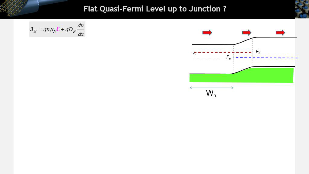
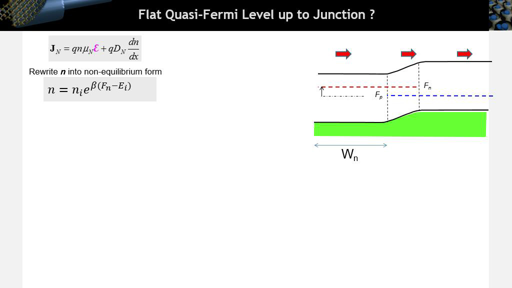
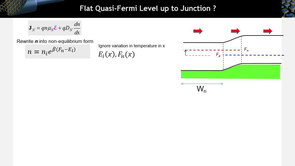
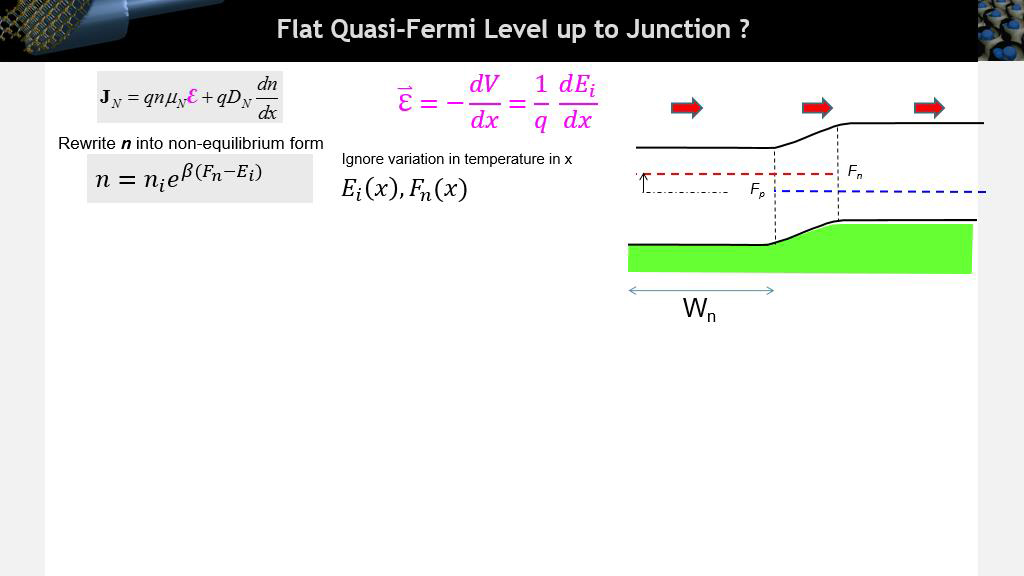
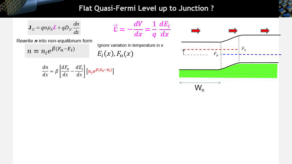
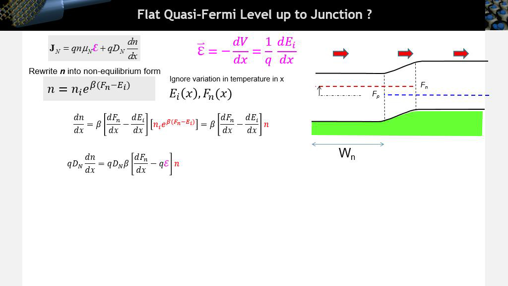
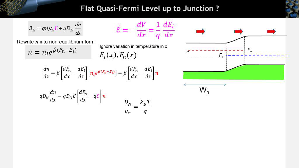
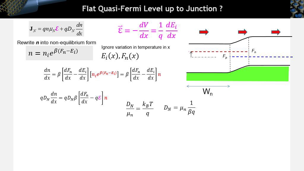
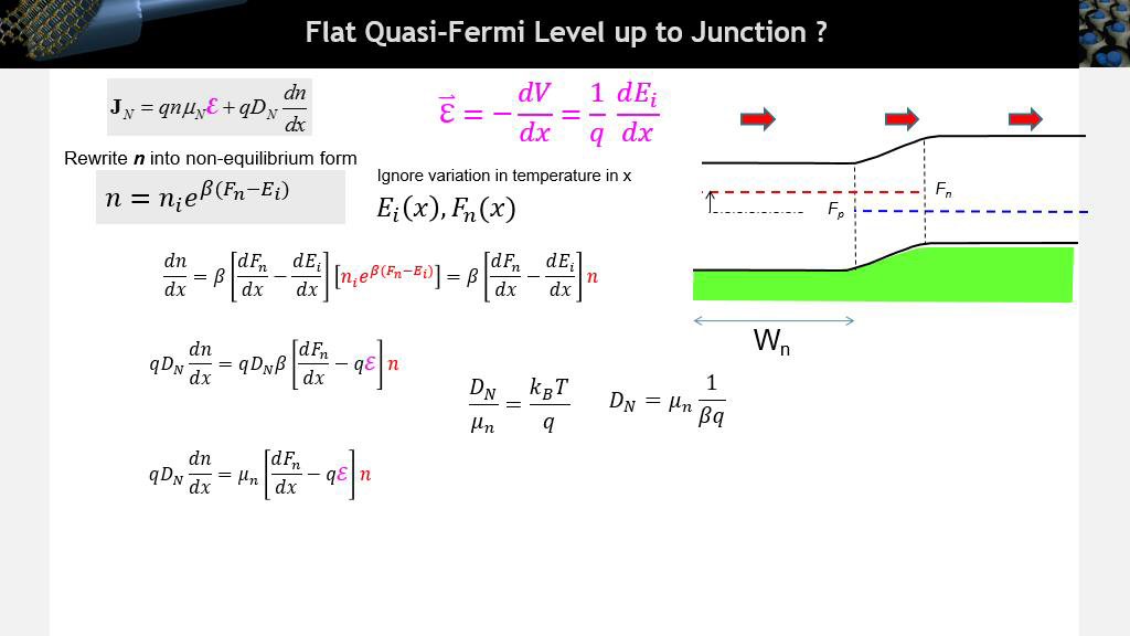
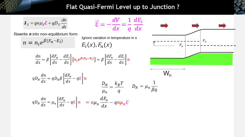
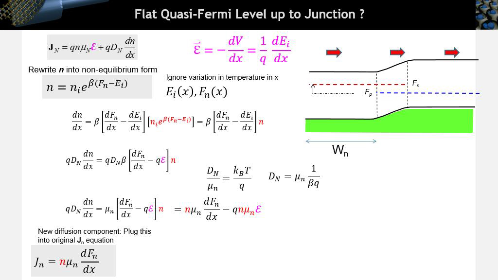
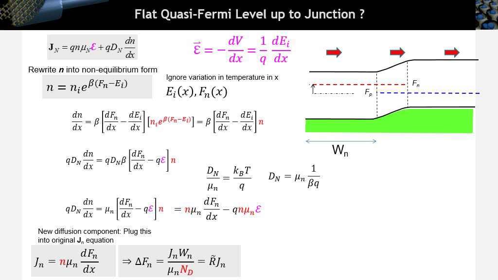
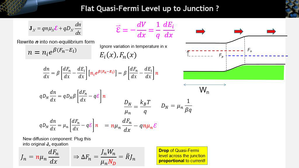
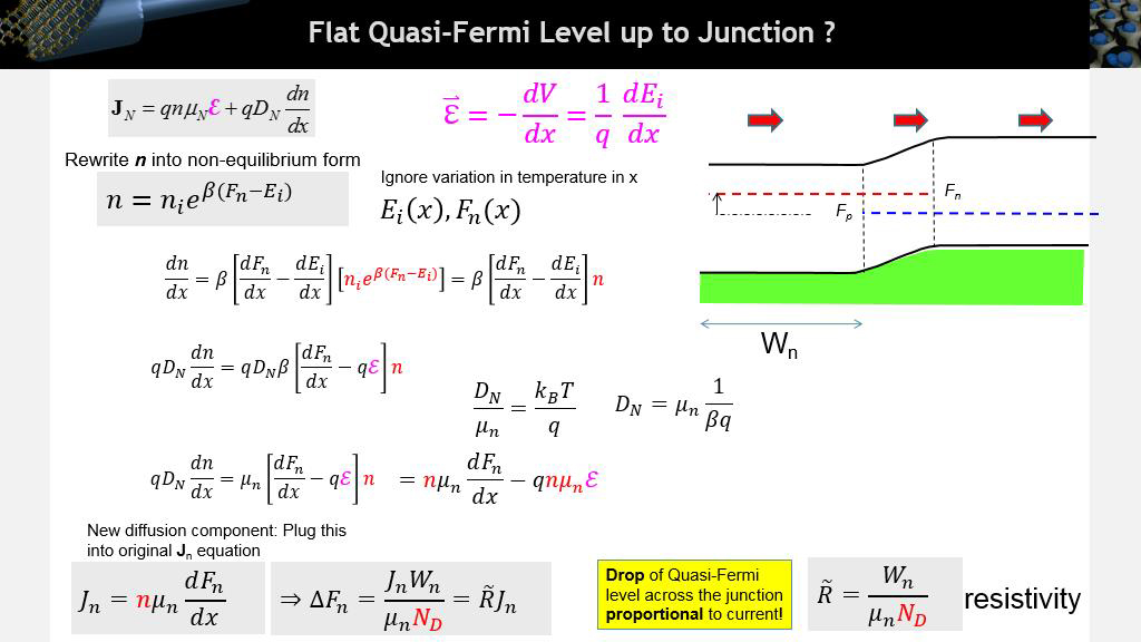 4. Flat Quasi-Fermi Level up to J…
156.79012345679013
00:00/00:00
4. Flat Quasi-Fermi Level up to J…
156.79012345679013
00:00/00:00 -
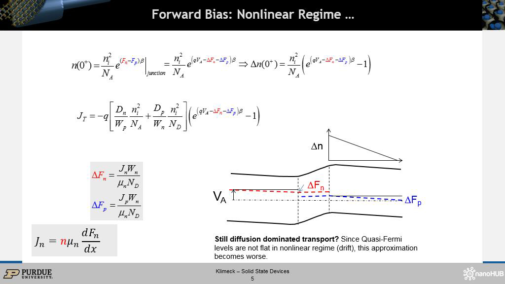 5. Forward Bias: Nonlinear Regime…
717.75108441775114
00:00/00:00
5. Forward Bias: Nonlinear Regime…
717.75108441775114
00:00/00:00 -
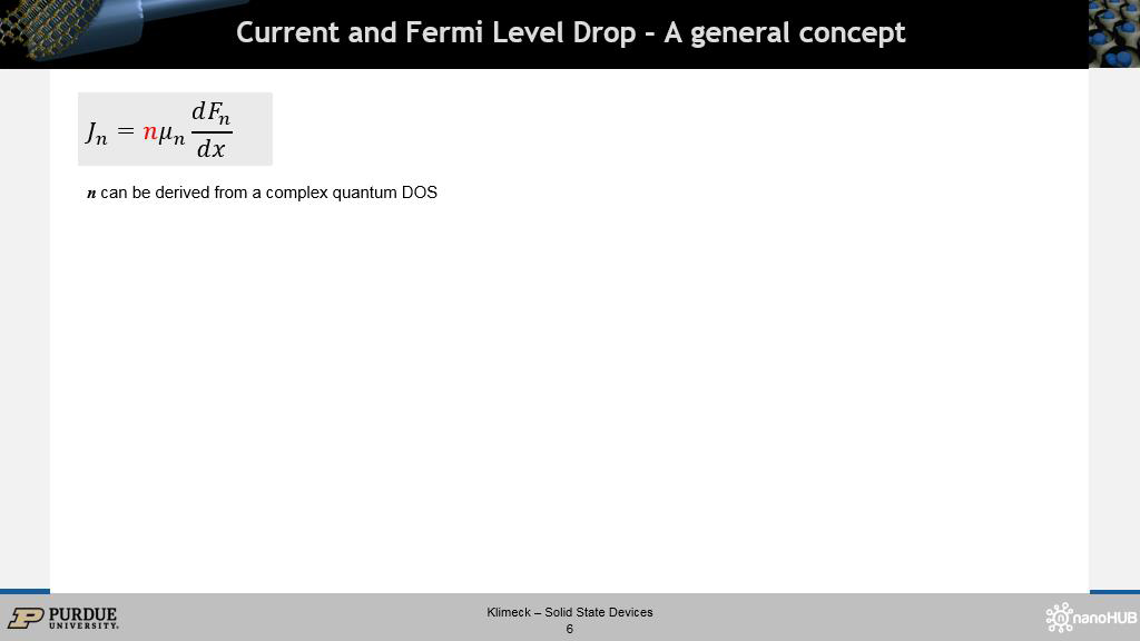
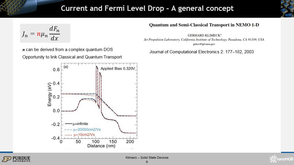
 6. Current and Fermi Level Drop �…
836.06940273606938
00:00/00:00
6. Current and Fermi Level Drop �…
836.06940273606938
00:00/00:00 -
 7. Section 20 PN Diode I-V Charac…
928.72872872872881
00:00/00:00
7. Section 20 PN Diode I-V Charac…
928.72872872872881
00:00/00:00 -
 8. Section 20 PN Diode I-V Charac…
935.1017684351018
00:00/00:00
8. Section 20 PN Diode I-V Charac…
935.1017684351018
00:00/00:00 -
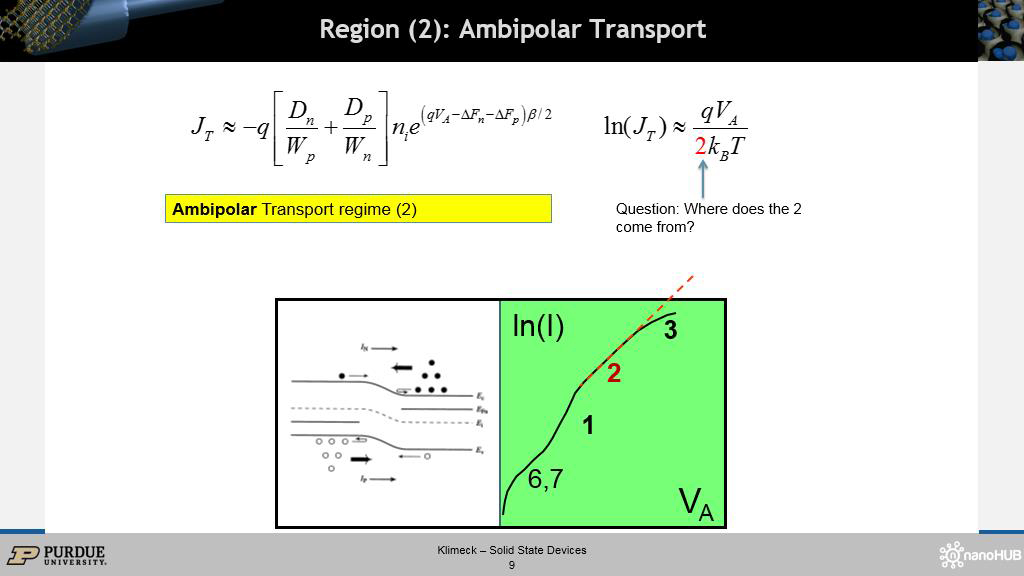 9. Region (2): Ambipolar Transpor…
937.37070403737073
00:00/00:00
9. Region (2): Ambipolar Transpor…
937.37070403737073
00:00/00:00 -
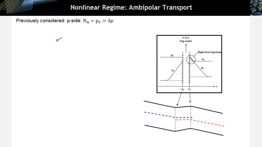
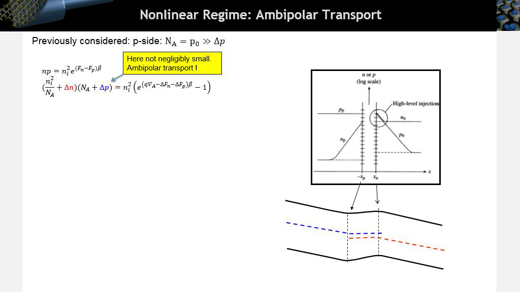
 10. Nonlinear Regime: Ambipolar Tr…
972.3056389723057
00:00/00:00
10. Nonlinear Regime: Ambipolar Tr…
972.3056389723057
00:00/00:00 -
 11. Region (2): Ambipolar Transpor…
1260.2936269602938
00:00/00:00
11. Region (2): Ambipolar Transpor…
1260.2936269602938
00:00/00:00 -
 12. Section 20 PN Diode I-V Charac…
1368.4017350684019
00:00/00:00
12. Section 20 PN Diode I-V Charac…
1368.4017350684019
00:00/00:00 -
 13. Section 20 PN Diode I-V Charac…
1378.7454120787454
00:00/00:00
13. Section 20 PN Diode I-V Charac…
1378.7454120787454
00:00/00:00