05 Ferroelectric Devices for Compute-in-Memory: Array-Level Operations
Category
Published on
Abstract
Day 2 Session 4.2, Invited Speaker
Abstract: Doped HfO2 based ferroelectric field-effect transistors (FeFETs) are being actively explored as emerging nonvolatile memory devices with the potential for compute-in-memory (CIM) paradigm. In this work, we explored the feasibility of array-level operations of FeFET in the context of in-situ training and inference for deep neural networks. To address the challenge of erase-by-block in NAND Flash structure, we proposed and experimentally demonstrated the drain erase scheme to enable the individual cell program/erase/inhibition, which is necessary for insitu training. The experimental conditions were characterized on 22nm FDSOI FeFET devices. A 3D timing sequence of weight update was designed and verified through 3D-array level SPICE simulation.
Introduction: Compute-in-memory (CIM) where the computation is directly performed within memory can avoid data communications between memory and processor, thus accelerating the deep neural network. Among the non-volatile memory candidates proposed for CIM, PCM and RRAM are challenging for in-situ training due to its asymmetry and high write energy [1]. Alternatively, HfxZr1-xO2 based FeFET [2] has been demonstrated symmetric multilevel channel conductance tuning and relatively lower write energy [3]. FeFET operates similarly as Flash with tunable threshold voltage (Vth), but it has lower write voltage (~3V) and shorter write latency (~50ns). A 4-layer 3D vertical channel FeFET prototype has been demonstrated [4]. However, one grand challenge remains to use 3D FeFET for in-situ training is the block-erase nature of the NAND array. The weight update rule in deep neural network requires each weight’s conductance could be independently tuned. This means the conventional substrate-erase scheme is not applicable as it will erase the entire block. In the recent published work [5-6], we proposed a 3D NAND-like FeFET array architecture feasible for both in-situ training and inference. To enable the individual cell program/erase, we experimentally demonstrated the feasibility of drain-erase scheme, i.e., flipping ferroelectric domain polarity by applying Verase to the drain to increase the channel potential and grounding the gate, on 22nm FDSOI FeFET [7] from GlobalFoundries (Fig.1).
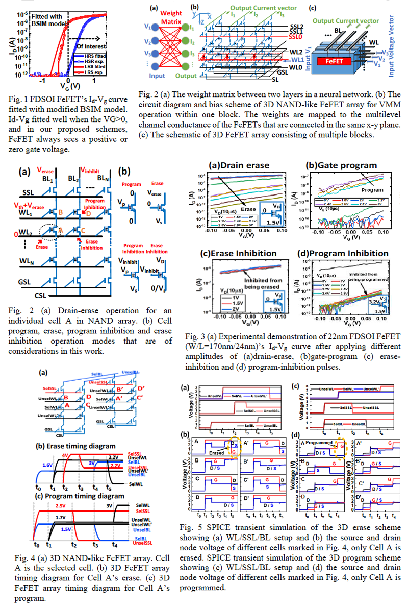
3D FeFET Array for CIM: Fig. 2 shows the circuit schematic of a 3D NAND-like FeFET array architecture. The top and bottom layers are select string transistors and ground select transistors. The gates of select string transistors in the same row (x-direction) are connected to the same string select line (SSL). All the gates of the bottom layers are connected by the ground select line (GSL). The middle are all vertical channel FeFETs, forming pillars in the z-direction. In each block, all the pillars in the y-direction share the same bit-line (BL), while all the gates of FeFETs in the same layer (x-y plane) are connected to the same word-line (WL) at the edge of the plane. BLs among different blocks are connected, while the WLs are independent among blocks (Fig. 1 (c)). When performing vector-matrix multiplication (VMM), the input vector is applied to WLs of multiple blocks from the x-direction to activate one layer, and BL currents are summed up along the y-direction from multiple blocks as the output, see discussions at [8].
FeFET Measurement: During the NAND write operation, the cell’s bias condition can be categorized into four modes: program mode, erase mode, programinhibition mode and erase-inhibition mode (Fig. 2). The experimental demonstration shows that the drain-erase is quite effective when the source is biased to 1.5V. The inhibition conditions of Cell C from being erased and Cell D from being programmed were also characterized, where the inhibition voltage in a range of 1~2 V/10μs is effective. (Fig. 3).
Simulations on 3D FeFET Array: To evaluate the feasibility of the drain-erase scheme to the 3D NANDlike FeFET array. The BSIM model was modified to fit the experimental programmed/erased FeFET Id-Vg curve (Fig. 1) and then was used for SPICE simulation for the 3D array. The timing sequence for individual cell’s erase and program in 3D NAND array is designed (Fig.4). To validate this scheme, a SPICE circuit simulation was performed with a 3D netlist for the array in transient mode to check the node voltage in each timing point (Fig. 5). The voltage waveform proves that only Cell A could be successfully erased during erase operation and all the other cells will not be disturbed due to insufficient node voltage differences. Similarly, during the program operation, Cell A receives 3V at the gate and 0V at the drain and source for effective gate programming, while other cells will not be disturbed.
Conclusion: 3D NAND-like FeFET array is proposed for both in-situ training and inference for deep neural network. We experimentally demonstrated the effectiveness of drain-erase scheme on 22nm FDSOI FeFET, which is the key technique to enable individual cell program/erase for independent weight-update. With the extracted BSIM model and specially designed timing sequence, the individual cell’s program/erase are successfully demonstrated through 3D array-level SPICE simulations.
Credits
We are grateful for Asif Khan and Globalfoundries. This work is in part supported by ASCENT, one of the SRC/DARPA JUMP centers.
Sponsored by
References
- S. Yu, Proc. IEEE, 2018.
- S. Dünkel et al., IEDM, 2017.
- M. Jerry et al. IEDM, 2017.
- K. Florent, et al., IEDM, 2018.
- P. Wang, et al., IEEE TED, vol. 67, no. 3, pp. 955-961, 2020.
- P. Wang, et al., IEEE TED, vol. 67, no. 3, pp. 962-967, 2020.
- S. Dünkel, et al., IEDM, 2017.
- P. Wang, et al., IEEE T-VLSI, vol. 27, no. 4, pp. 988-991, 2019.
Cite this work
Researchers should cite this work as follows:
Time
Location
DRC 2020 Virtual Conference