05 Ferroelectric Devices for Compute-in-Memory: Array-Level Operations
Ferroelectric Devices for Compute-in-Memory: Array-Level Operations
-
 1. Ferroelectric Devices for Comp…
0
00:00/00:00
1. Ferroelectric Devices for Comp…
0
00:00/00:00 -
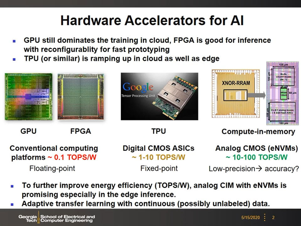 2. Hardware Accelerators for AI
13.513513513513514
00:00/00:00
2. Hardware Accelerators for AI
13.513513513513514
00:00/00:00 -
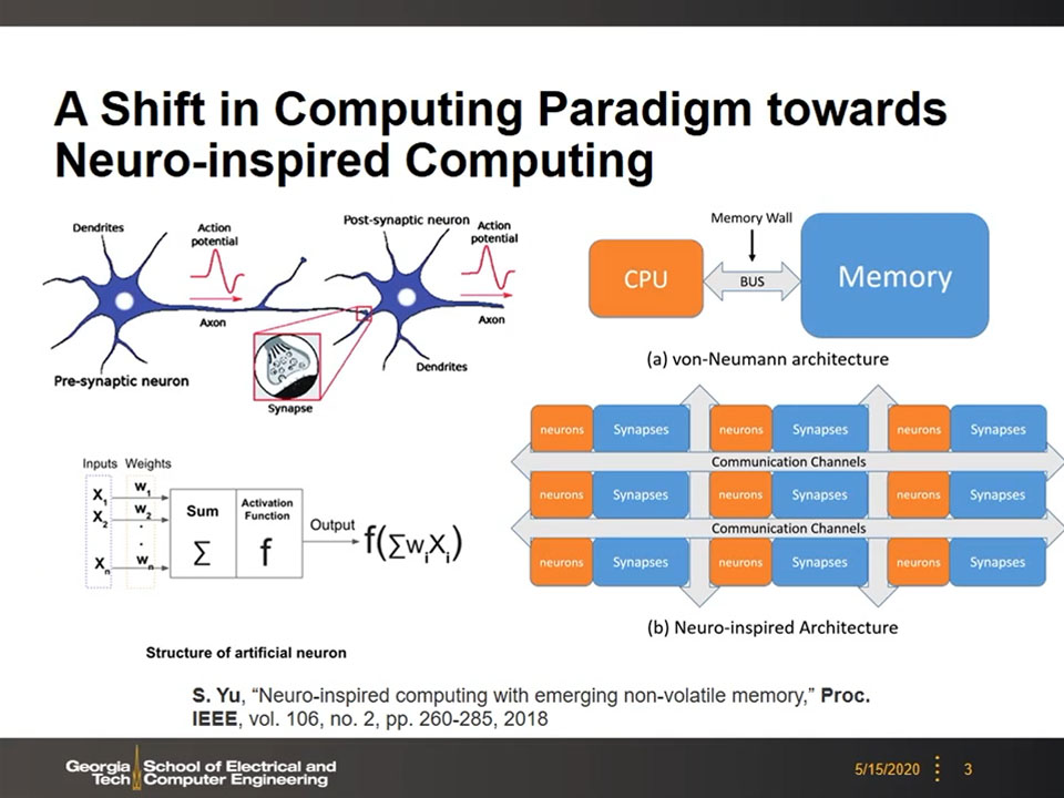 3. A Shift in Computing Paradigm …
174.70804137470805
00:00/00:00
3. A Shift in Computing Paradigm …
174.70804137470805
00:00/00:00 -
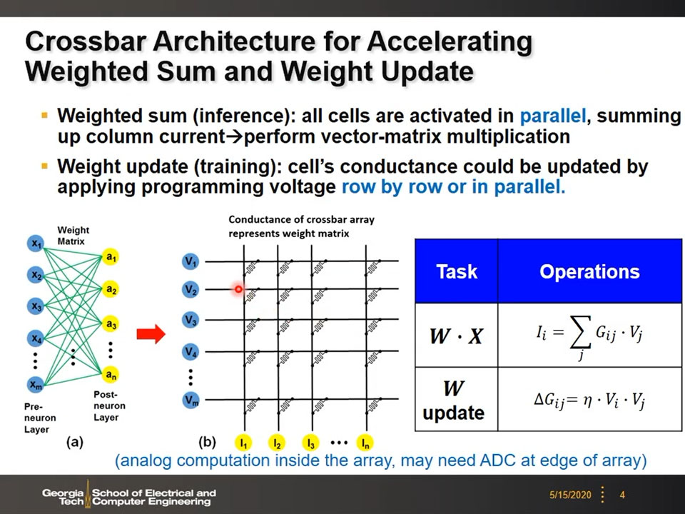 4. Crossbar Architecture for Acce…
300.70070070070074
00:00/00:00
4. Crossbar Architecture for Acce…
300.70070070070074
00:00/00:00 -
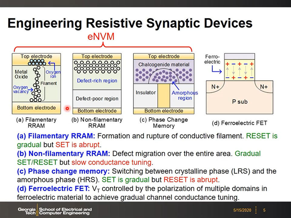 5. Engineering Resistive Synaptic…
406.47313980647317
00:00/00:00
5. Engineering Resistive Synaptic…
406.47313980647317
00:00/00:00 -
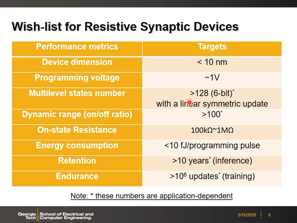 6. Wish-list for Resistive Synapt…
545.51217884551215
00:00/00:00
6. Wish-list for Resistive Synapt…
545.51217884551215
00:00/00:00 -
 7. Questions?
736.10276943610279
00:00/00:00
7. Questions?
736.10276943610279
00:00/00:00 -
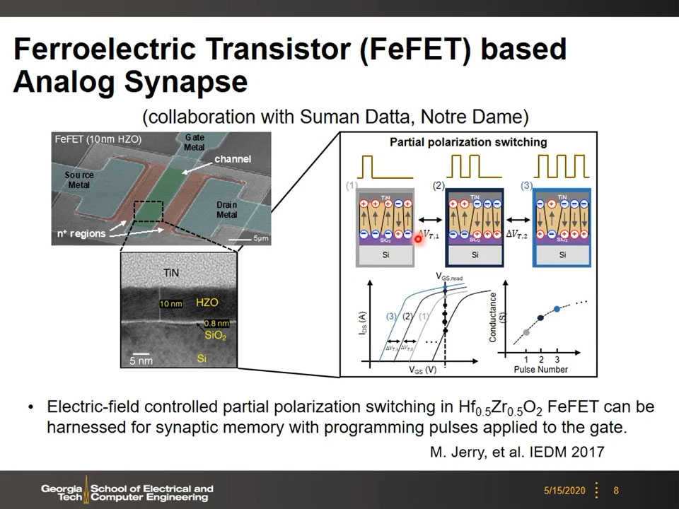 8. Ferroelectric Transistor (FeFE…
741.10777444110784
00:00/00:00
8. Ferroelectric Transistor (FeFE…
741.10777444110784
00:00/00:00 -
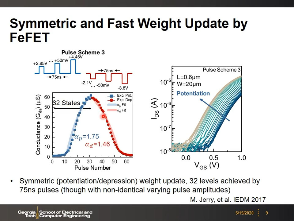 9. Symmetric and Fast Weight Upda…
822.18885552218887
00:00/00:00
9. Symmetric and Fast Weight Upda…
822.18885552218887
00:00/00:00 -
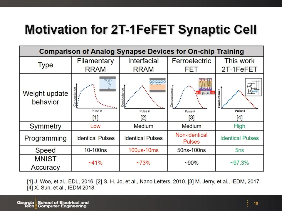 10. Motivation for 2T-1FeFET Synap…
873.03970637303973
00:00/00:00
10. Motivation for 2T-1FeFET Synap…
873.03970637303973
00:00/00:00 -
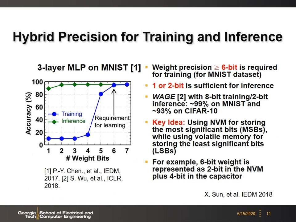 11. Hybrid Precision for Training …
996.62996329663
00:00/00:00
11. Hybrid Precision for Training …
996.62996329663
00:00/00:00 -
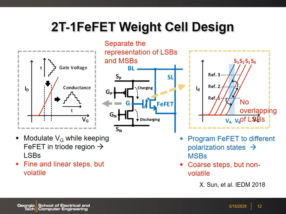 12. 2T-1FeFET Weight Cell Design
1105.2052052052052
00:00/00:00
12. 2T-1FeFET Weight Cell Design
1105.2052052052052
00:00/00:00 -
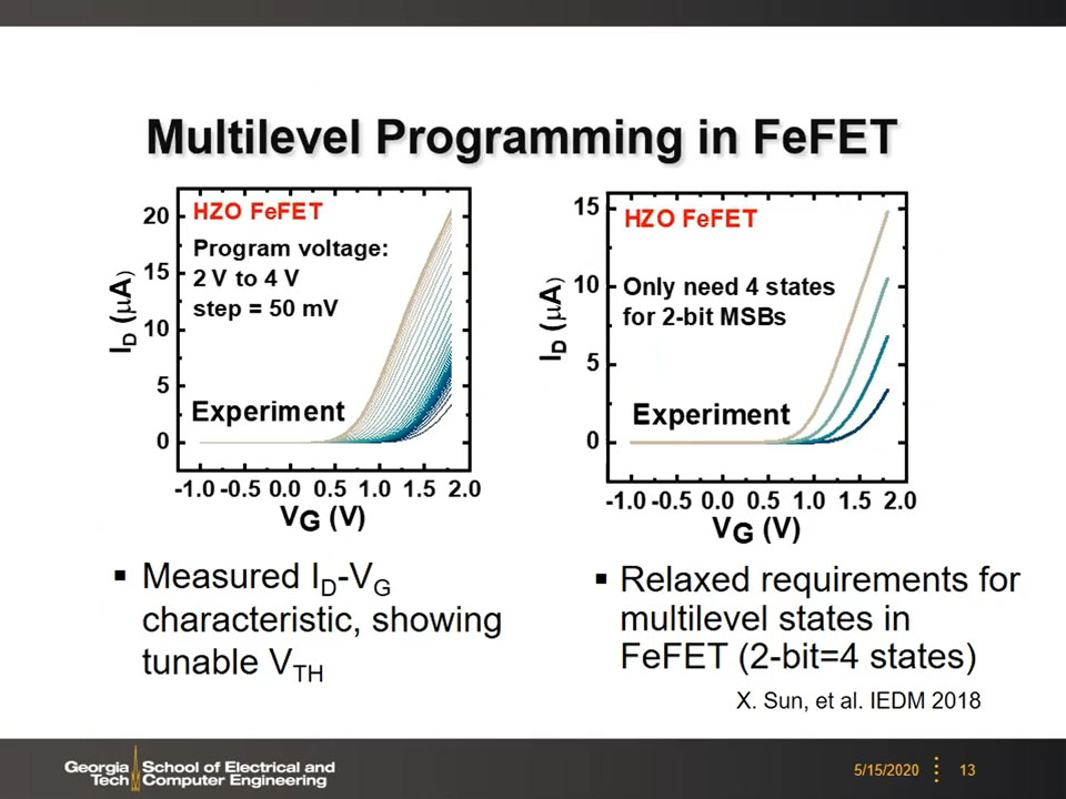 13. Multilevel Programming in FeFE…
1316.7500834167502
00:00/00:00
13. Multilevel Programming in FeFE…
1316.7500834167502
00:00/00:00 -
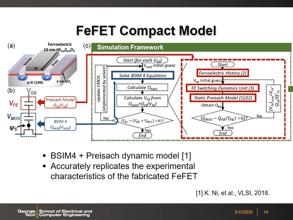 14. FeFET Compact Model
1351.217884551218
00:00/00:00
14. FeFET Compact Model
1351.217884551218
00:00/00:00 -
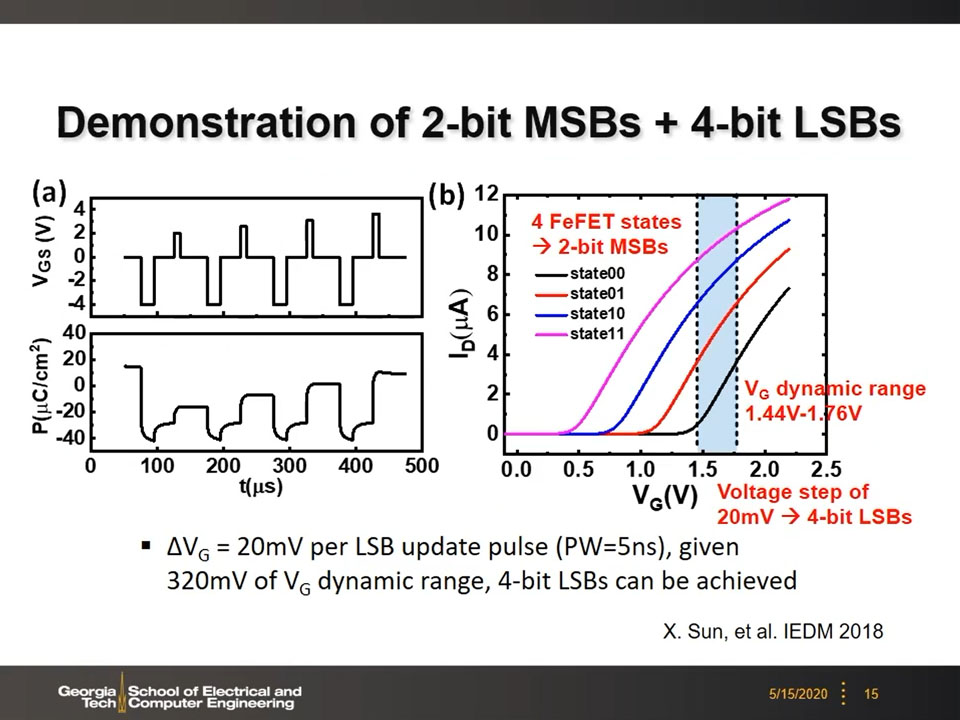 15. Demonstration of 2-bit MSBs + …
1389.2225558892226
00:00/00:00
15. Demonstration of 2-bit MSBs + …
1389.2225558892226
00:00/00:00 -
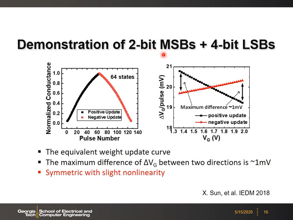 16. Demonstration of 2-bit MSBs + …
1430.8308308308308
00:00/00:00
16. Demonstration of 2-bit MSBs + …
1430.8308308308308
00:00/00:00 -
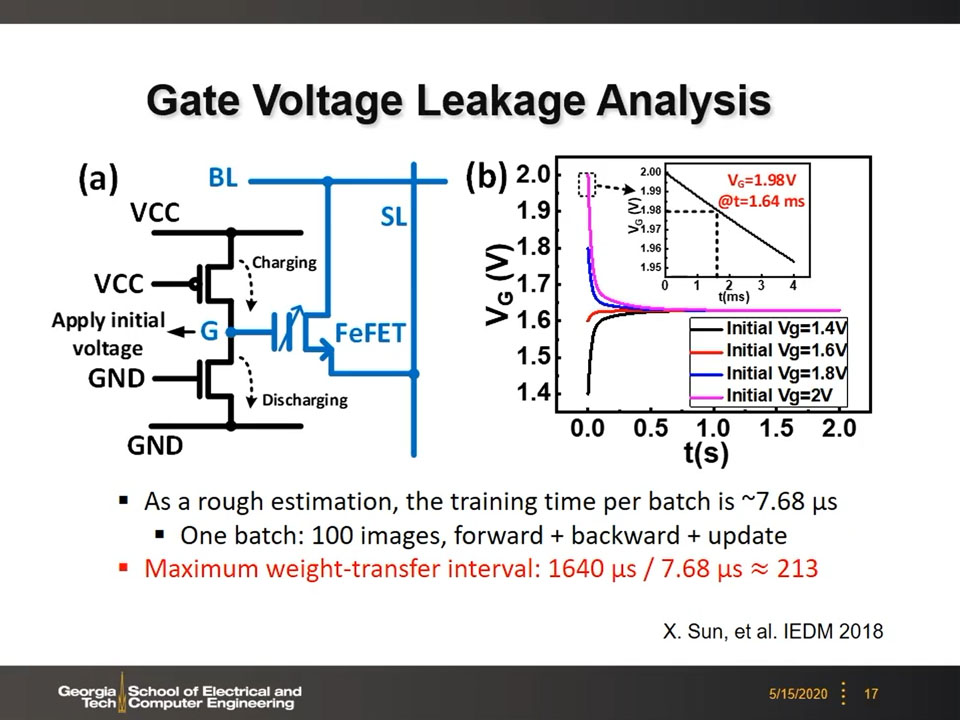 17. Gate Voltage Leakage Analysis
1477.6776776776778
00:00/00:00
17. Gate Voltage Leakage Analysis
1477.6776776776778
00:00/00:00 -
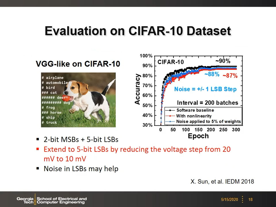 18. Evaluation on CIFAR-10 Dataset
1532.6326326326327
00:00/00:00
18. Evaluation on CIFAR-10 Dataset
1532.6326326326327
00:00/00:00 -
 19. Questions?
1584.3510176843511
00:00/00:00
19. Questions?
1584.3510176843511
00:00/00:00 -
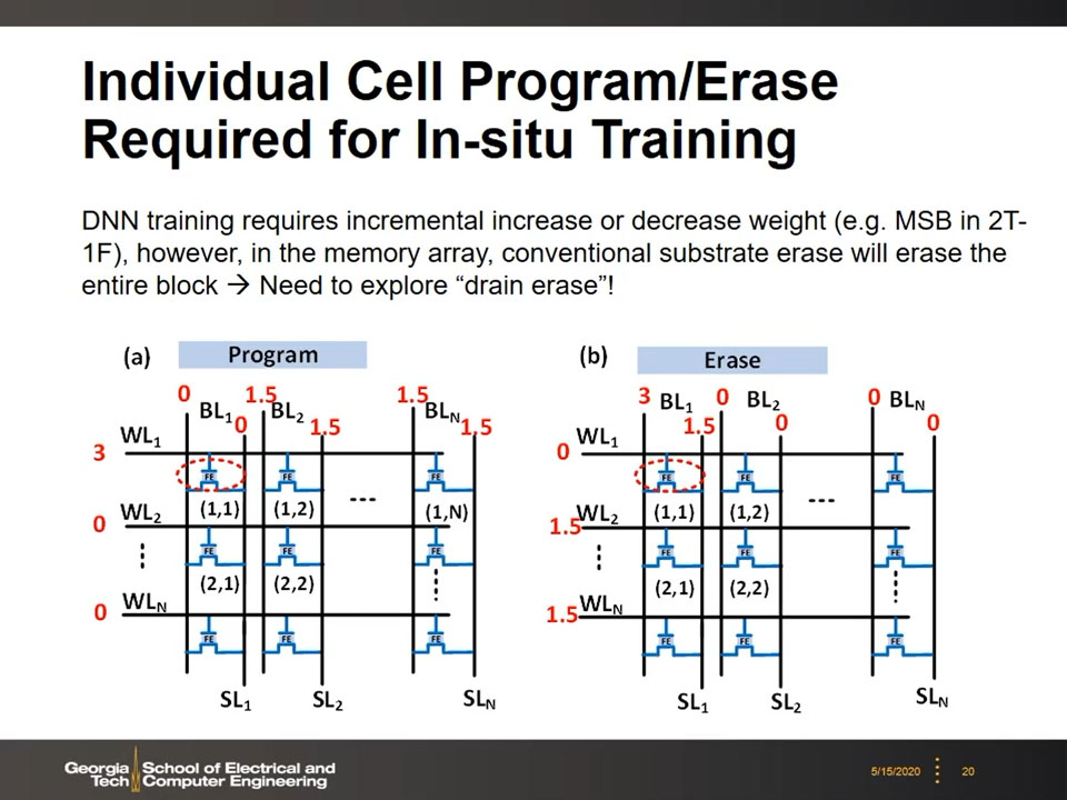 20. Individual Cell Program/Erase …
1589.356022689356
00:00/00:00
20. Individual Cell Program/Erase …
1589.356022689356
00:00/00:00 -
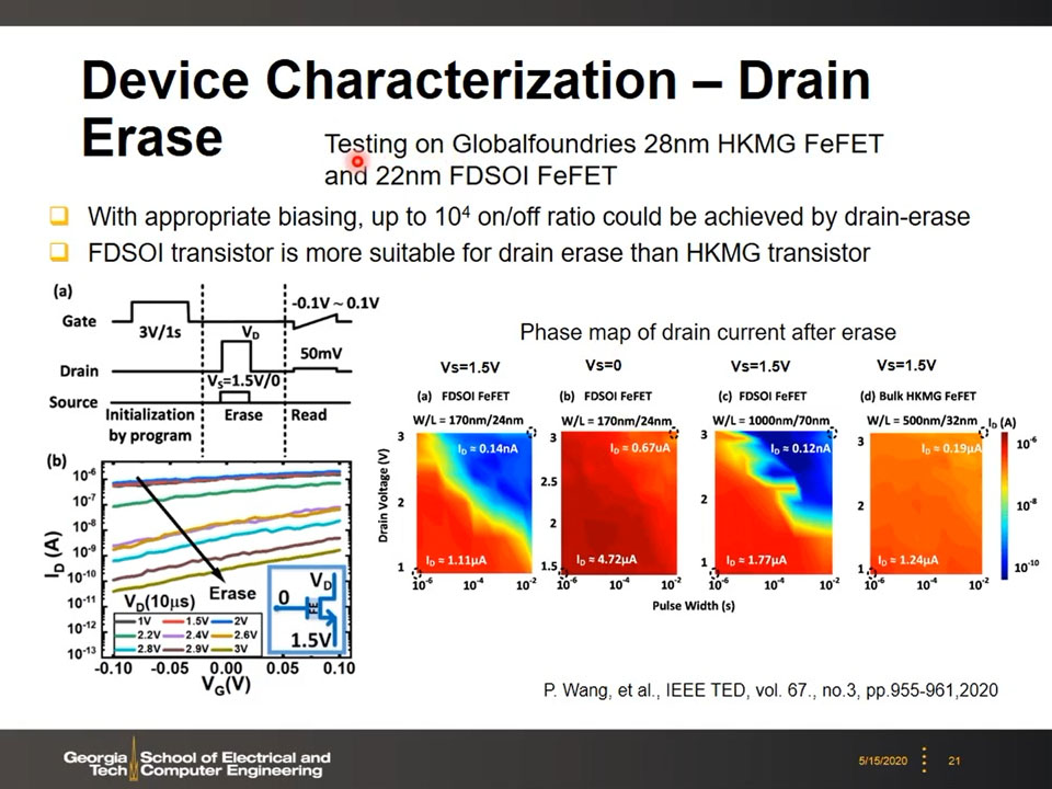 21. Device Characterization – Dr…
1764.7313980647314
00:00/00:00
21. Device Characterization – Dr…
1764.7313980647314
00:00/00:00 -
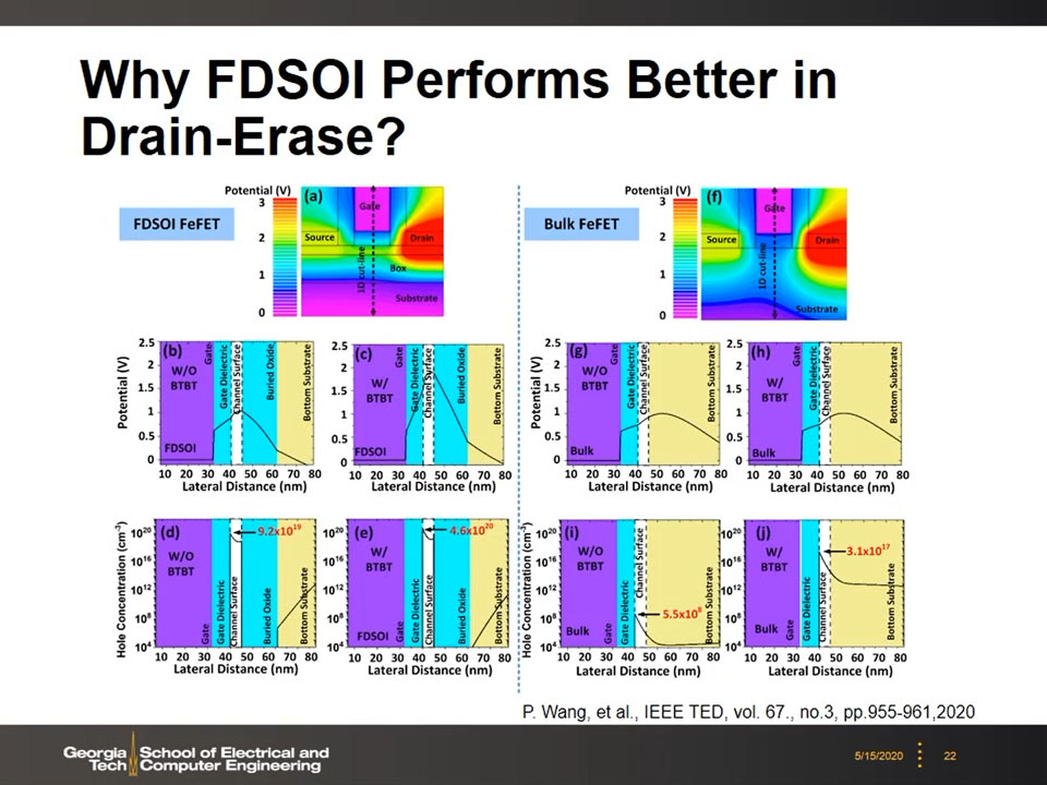 22. Why FDSOI Performs Better in D…
1878.9122455789122
00:00/00:00
22. Why FDSOI Performs Better in D…
1878.9122455789122
00:00/00:00 -
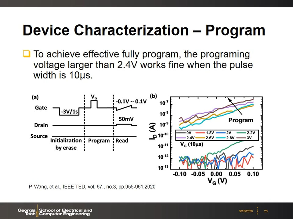 23. Device Characterization – Pr…
1931.0977644310979
00:00/00:00
23. Device Characterization – Pr…
1931.0977644310979
00:00/00:00 -
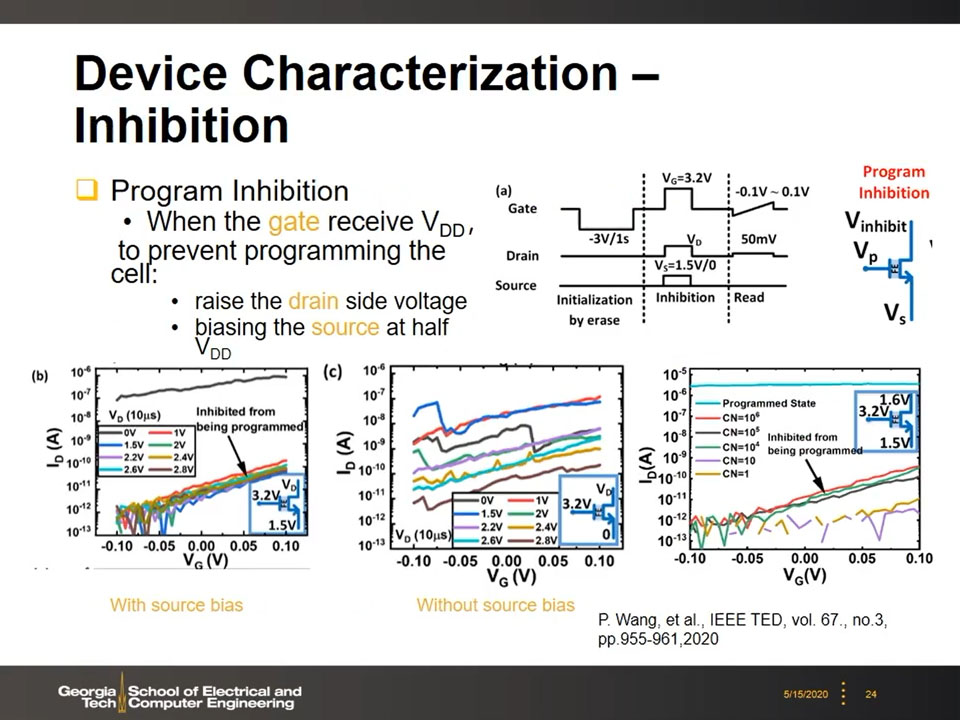 24. Device Characterization – In…
1965.4320987654321
00:00/00:00
24. Device Characterization – In…
1965.4320987654321
00:00/00:00 -
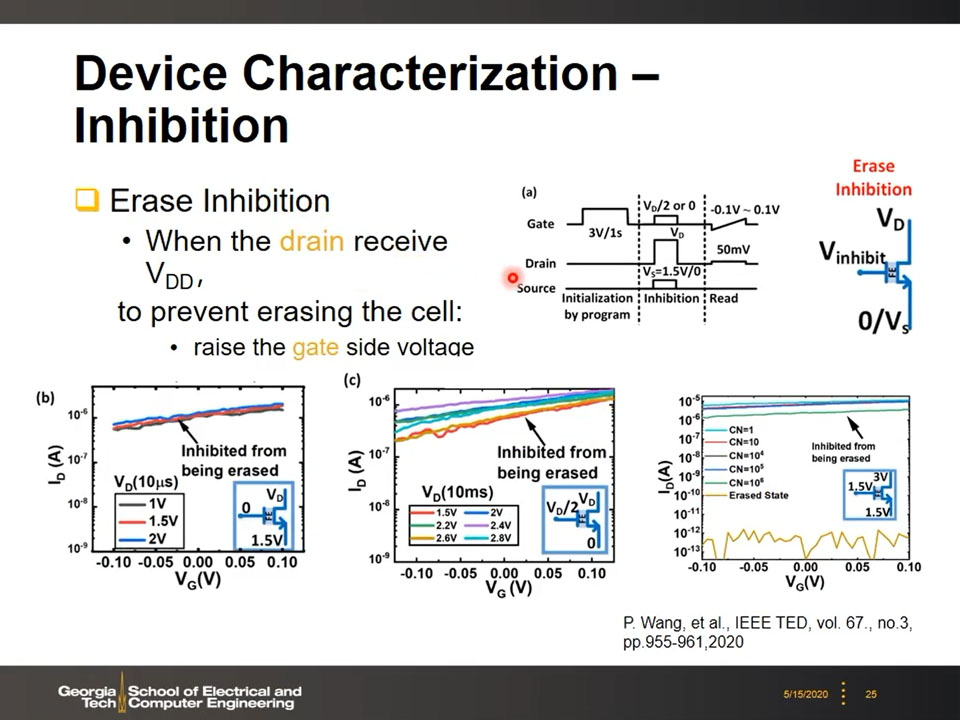 25. Device Characterization – In…
2046.47981314648
00:00/00:00
25. Device Characterization – In…
2046.47981314648
00:00/00:00 -
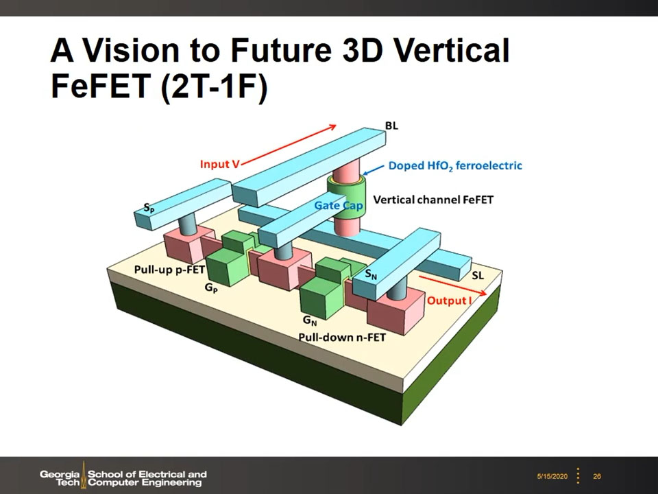 26. A Vision to Future 3D Vertical…
2065.6990323656992
00:00/00:00
26. A Vision to Future 3D Vertical…
2065.6990323656992
00:00/00:00 -
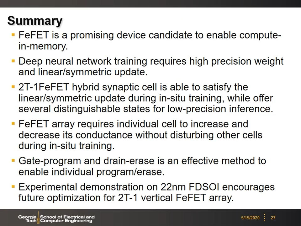 27. Summary
2122.0220220220222
00:00/00:00
27. Summary
2122.0220220220222
00:00/00:00 -
 28. Acknowledgement
2175.608942275609
00:00/00:00
28. Acknowledgement
2175.608942275609
00:00/00:00