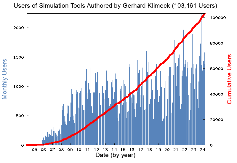
Your Career Choices: A Perspective from 24 years in Industry, National Laboratory, and Academia and The Most-Neglected Item in your Career Development
02 Jul 2018 | Online Presentations | Contributor(s): Gerhard Klimeck
What are your career choices with a BS, MS, or PhD? Will you develop technology yourself? Will you work in a team? Will you guide people? Where will you work: in industry, research lab, or academia?
Your Career Choices after Graduate School and The Most-Neglected Item in your Career Development (2016)
20 Sep 2016 | Online Presentations | Contributor(s): Gerhard Klimeck
What are your career choices after graduate school? Will you develop technology yourself? Will you work in a team? Will you guide people? Where will you work: in industry, research lab, or academia? Regardless where you work, there is generally one item that you are not being taught in graduate...
Your Career Choices after Graduate School and The Most-Neglected Item in your Career Development (2015)
23 Oct 2009 | Online Presentations | Contributor(s): Gerhard Klimeck
Worked Examples for Carrier Statistics (basic)
16 Aug 2010 | Teaching Materials | Contributor(s): Saumitra Raj Mehrotra, Dragica Vasileska, Gerhard Klimeck
Several worked out examples are presented that illustrate the basic concept of carrier concentration in semiconductors.
Worked Examples for a PN Diode
01 Jun 2010 | Teaching Materials | Contributor(s): Dragica Vasileska, Gerhard Klimeck
several worked examples are presented that illustrate the operation of a PN diode.
Why QuaMC 2D and Particle-Based Device Simulators?
0.0 out of 5 stars
02 May 2008 | Online Presentations | Contributor(s): Dragica Vasileska, Shaikh S. Ahmed, Gerhard Klimeck
We describe the need for particle-based device simulators when modeling nanoscale devices.
Why is Nanotechnology Multidisciplinary? A perspective of one EE
5.0 out of 5 stars
19 Oct 2006 | Online Presentations | Contributor(s): Gerhard Klimeck
The field of nano science and nano-technology covers broad areas of expertise. Classical fields of Physics, Chemistry, Material Science, Electrical/Mechanical/Chemical Engineering all are involved in the "new" field. Nano research and development is therefore multidisciplinary. This...
What are the proper transport models at the nanoscale?
29 Jun 2011 | Teaching Materials | Contributor(s): Dragica Vasileska, Gerhard Klimeck
This presentation is part of the series Nanoelectronics and Modeling at the Nanoscale
Verification of the Validity of the PN Junction Tool
05 Jun 2010 | Teaching Materials | Contributor(s): Dragica Vasileska, Gerhard Klimeck
These simulations and comparisons with the depletion charge approximation prove the validity of the PN Junction tool.
Verification of the Validity of the MOSFET Tool
10 Oct 2010 | Teaching Materials | Contributor(s): Saumitra Raj Mehrotra, Dragica Vasileska, Gerhard Klimeck
Output characteristics of a bulk MOSFET are computed using MOSFET lab and compared with an analytical model based on Bulk-Charge theory. Parasitic resistance is used as a fitting parameter in the analytical model. MATLAB script used for verification is also available for download.
Verification of the Validity of the MOSCap Tool
10 Aug 2010 | Teaching Materials | Contributor(s): Saumitra Raj Mehrotra, Dragica Vasileska, Gerhard Klimeck
Numerical results for Surface Potential Vs Gate Bias are compared with analytical results to prove the validity of MOSCap Lab.
Verification of the Validity of the Drift-Diffusion Lab Tool
Drift-Diffusion Lab results are verified analytically. In the first test minority carrier concentration is computed in a semiconductor slab with constant carrier Generation rate (/cm3.s). In the second test bias is applied across a semiconductor slab and current is computed both analytically and...
Verification of the Validity of the BJT Tool
22 Aug 2010 | Teaching Materials | Contributor(s): Saumitra Raj Mehrotra, Dragica Vasileska, Gerhard Klimeck
A pnp BJT in Common-Base configuration is analyzed both analytically and numerically using BJT Lab. DC current gain and Output characteristics are computed.MATLAB script used is also available for download.
Verification of the Validity of Bulk Bandstructure Lab
09 Aug 2010 | Teaching Materials | Contributor(s): Dragica Vasileska, Gerhard Klimeck
This set of slides compares the optical gaps for Si, Ge and GaAs with those given in www.ioffe.ru, thus verifying the validity of the bulk Bandstructure Lab tool.
Valley splitting in strained silicon quantum wells modeled with 2 degree miscuts, step disorder, and alloy disorder
14 Jan 2008 | Papers | Contributor(s): Neerav Kharche, marta prada, Timothy Boykin, Gerhard Klimeck
Valley splitting (VS) in strained SiGe/Si/SiGe quantum wells grown on (001) and 2° miscut substrates is computed in a magnetic field. Calculations of flat structures significantly overestimate, while calculations of perfectly ordered structures underestimate experimentally observed VS. Step...
Universal Behavior of Strain in Self-assembled Quantum Dots
01 May 2016 | Downloads | Contributor(s): Hesameddin Ilatikhameneh, Tarek Ahmed Ameen, Gerhard Klimeck, Rajib Rahman
This resource contains the universal behavior strain files produced by Nemo5. Attached also a Matlab script that can utilize the these compact descriptive files to produce the full strain distribution. Supported QD shapes; Cuboid, Dome, Cone, and Pyramid. Supported material systems;...
Uniform versus delta doping in 1D heterostructures: an Exercise
15 Aug 2008 | Teaching Materials | Contributor(s): Dragica Vasileska, Gerhard Klimeck
This exercise is designed to demonstrate that delta doping leads to larger sheet electron density in the channel and it also allows for better control of the charge density in the channel region of High Electron Mobility Transistors (HEMTs).
Tutorial for PADRE Based Simulation Tools
10 Aug 2009 | Teaching Materials | Contributor(s): Dragica Vasileska, Gerhard Klimeck
This tutorial is intended for first time and medium level users of PADRE-based simulation modules installed on the nanohub. It gives clear overview on the capabilities of each tool with emphasis to most important effects occuring in nano-scale devices.
Tutorial 4d: Formation of Bandstructure in Finite Superlattices (Exercise Demo)
23 Mar 2011 | Online Presentations | Contributor(s): Gerhard Klimeck
Demonstration of thePiece-Wise Constant Potential Barriers Tool.
Tutorial 4c: Formation of Bandstructure in Finite Superlattices (Exercise Session)
How does bandstructure occur? How large does a repeated system have to be? How does a finite superlattice compare to an infinite superlattice?
Tutorial 4b: Introduction to the NEMO3D Tool - Electronic Structure and Transport in 3D
Electronic Structure and Transport in 3D - Quantum Dots, Nanowires and Ultra-Thin Body Transistors
Tutorial 4a: High Bias Quantum Transport in Resonant Tunneling Diodes
Outline:Resonant Tunneling Diodes - NEMO1D: Motivation / History / Key InsightsOpen 1D Systems: Transmission through Double Barrier Structures - Resonant TunnelingIntroduction to RTDs: Linear Potential DropIntroduction to RTDs: Realistic Doping ProfilesIntroduction to RTDs: Relaxation Scattering...
Tutorial 4: Far-From-Equilibrium Quantum Transport
23 Mar 2011 | Courses | Contributor(s): Gerhard Klimeck
These lectures focus on the application of the theories using the nanoelectronic modeling tools NEMO 1- D, NEMO 3-D, and OMEN to realistically extended devices. Topics to be covered are realistic resonant tunneling diodes, quantum dots, nanowires, and Ultra-Thin-Body Transistors.
Tunneling Through Triangular Barrier: an Exercise for PCPBT
23 Jul 2008 | Teaching Materials | Contributor(s): Dragica Vasileska, Gerhard Klimeck
This exercise teaches the users that a very good result can be obtained when the triangular barrier is approximated with 11 segment piece-wise constant potential barrier steps. www.eas.asu.edu/~vasilesk NSF
Tunneling in an Nanometer-Scaled Transistor
25 Jan 2011 | Animations | Contributor(s): Gerhard Klimeck, Mathieu Luisier, Neerav Kharche, George A. Howlett, Insoo Woo, David Ebert
Electrons tunneling through the gate of an ultra-scaled transistor.