ABACUS Tool Suite and Bulk Semiconductors (Fall 2023)
Category
Published on
Abstract
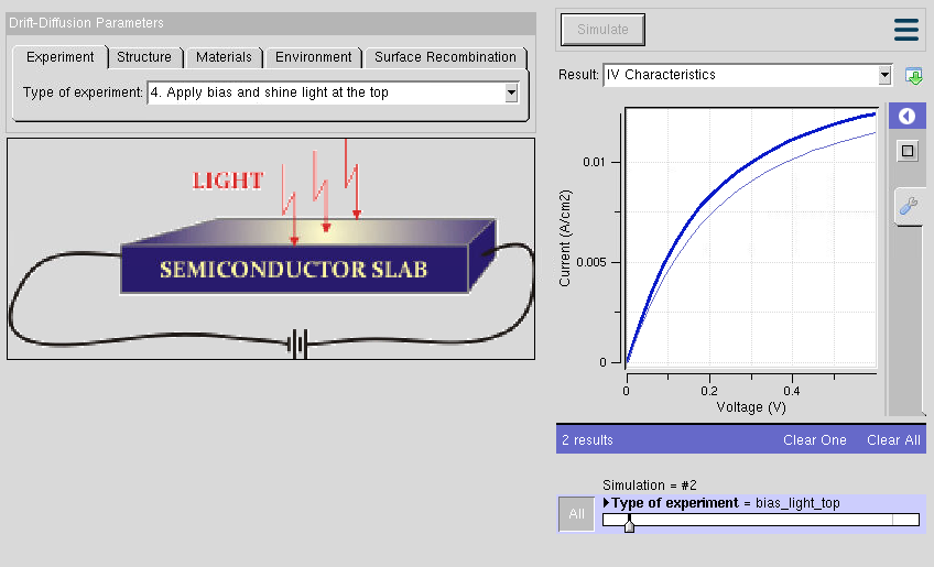
 In the third session, Dr. Klimeck will give a brief overview of ABACUS and demonstrate the Drift-Diffusion-Lab. Students can experiment with a semiconductor slab under bias and/or light illumination. They can explore how illumination from the top of an intrinsic semiconductor increases the overall current and separates the hole and electron distribution across the device. They can change the light intensity and the location of the illumination. Different materials such as Si, SiGe, and GaAs can be explored. Detailed parameters such as minority carrier lifetimes or surface recombination times can be modified in numerical experiments to explore the concepts. Drift-Diffusion-Lab is powered by the industrial tool PADRE which was used at Bell Labs to design transistors.
Earlier versions of this presentation can be found here: Winter 2021, and Spring 2022
Sponsored by
Cite this work
Researchers should cite this work as follows: