Nano-Characterization and Nano-Fabrication using EB/IB Tools
 Tomoko Borsa was born in Tokyo, Japan and completed a BS and MS at Waseda University, where she was exposed to the field of scanning electron microscopy for the first time. She then earned a Ph.D. in Materials Science with an emphasis on Chemistry of Materials from Colorado School of Mines. She also received an MS in Electrical Engineering (Photonics and Nanostructures) from University of Colorado Boulder. She also has extensive experience in the area of micro/nanofabrication including electron beam lithography and related process development.
Nano-Characterization and Nano-Fabrication using EB/IB Tools
-
 1. Nano-Characterization and Nano…
0
00:00/00:00
1. Nano-Characterization and Nano…
0
00:00/00:00 -
 2. Table of Contents
86.086086086086084
00:00/00:00
2. Table of Contents
86.086086086086084
00:00/00:00 -
 3. Introduction to "Nano-World"
154.45445445445446
00:00/00:00
3. Introduction to "Nano-World"
154.45445445445446
00:00/00:00 -
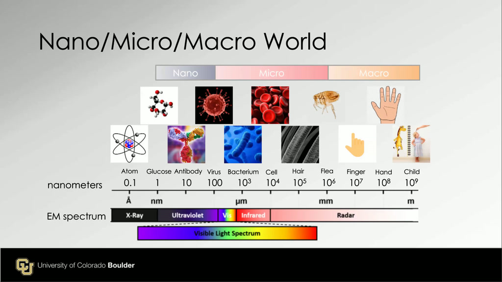 4. Nano/Micro/Macro World
220.58725392058727
00:00/00:00
4. Nano/Micro/Macro World
220.58725392058727
00:00/00:00 -
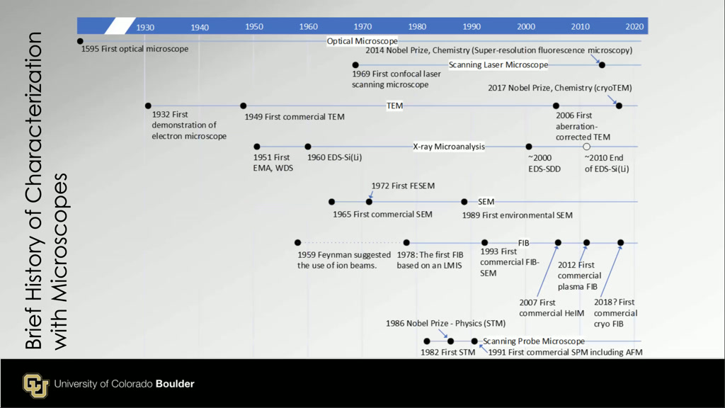 5. Brief History of Characterizat…
382.48248248248251
00:00/00:00
5. Brief History of Characterizat…
382.48248248248251
00:00/00:00 -
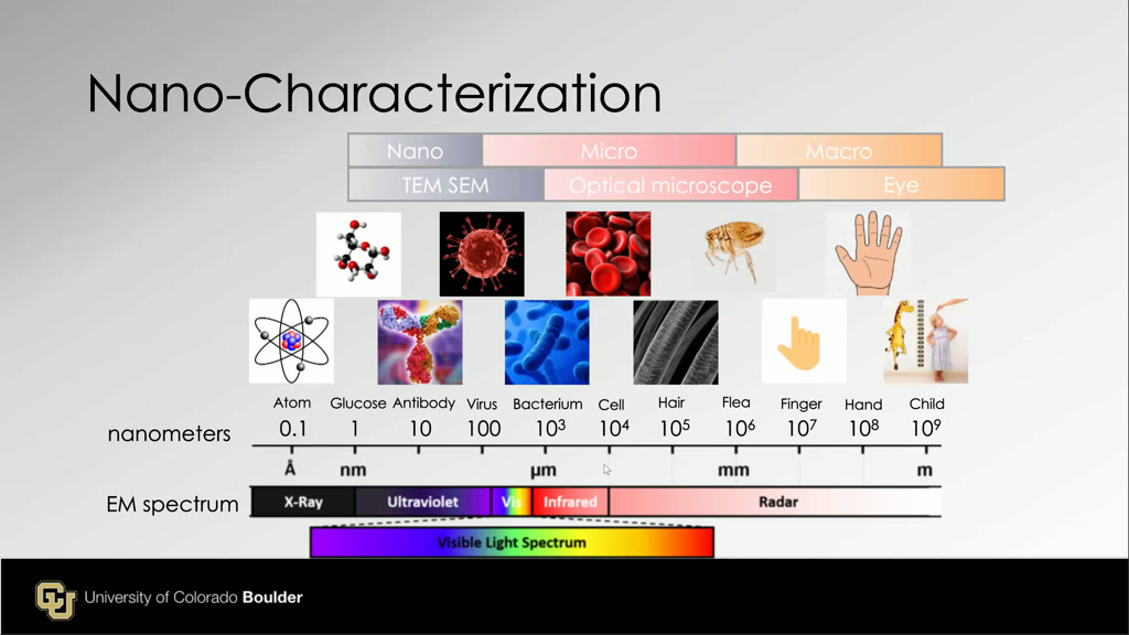 6. Nano-Characterization
707.90790790790788
00:00/00:00
6. Nano-Characterization
707.90790790790788
00:00/00:00 -
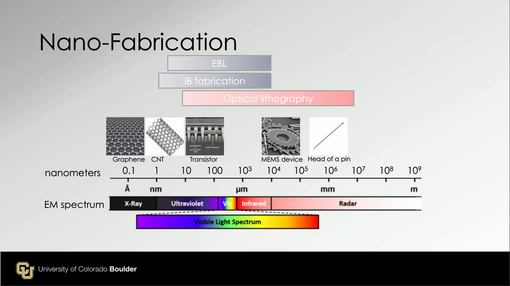 7. Nano-Fabrication
745.64564564564569
00:00/00:00
7. Nano-Fabrication
745.64564564564569
00:00/00:00 -
 8. Semiconductor History
943.51017684351018
00:00/00:00
8. Semiconductor History
943.51017684351018
00:00/00:00 -
 9. MOSFET Scaling
1040.4738071404738
00:00/00:00
9. MOSFET Scaling
1040.4738071404738
00:00/00:00 -
 10. Optical Lithography
1175.3753753753754
00:00/00:00
10. Optical Lithography
1175.3753753753754
00:00/00:00 -
 11. Optical Lithography
1284.4177510844179
00:00/00:00
11. Optical Lithography
1284.4177510844179
00:00/00:00 -
 12. DUV and EUV Lithography
1365.1317984651319
00:00/00:00
12. DUV and EUV Lithography
1365.1317984651319
00:00/00:00 -
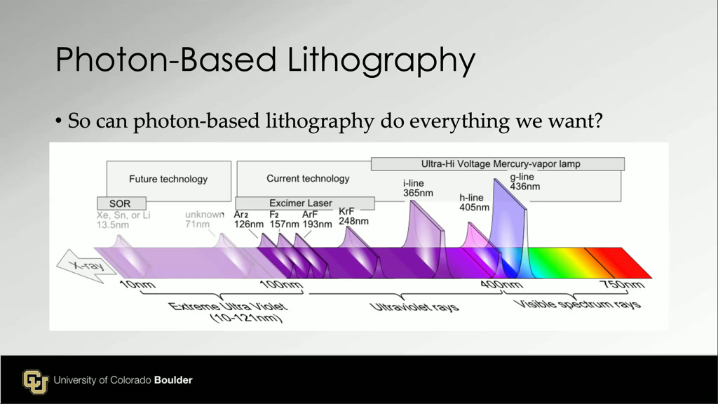 13. Photon-Based Lithography
1504.1041041041042
00:00/00:00
13. Photon-Based Lithography
1504.1041041041042
00:00/00:00 -
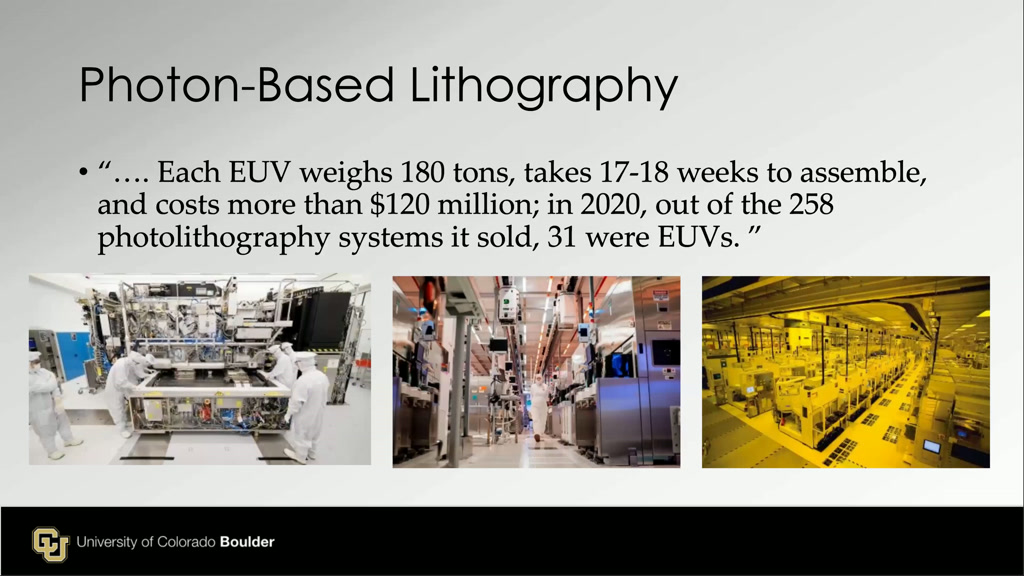 14. Photon-Based Lithography
1530.4304304304305
00:00/00:00
14. Photon-Based Lithography
1530.4304304304305
00:00/00:00 -
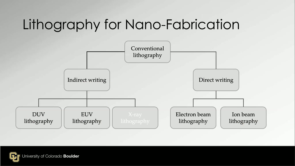 15. Lithography for Nano-Fabricati…
1596.2295628962297
00:00/00:00
15. Lithography for Nano-Fabricati…
1596.2295628962297
00:00/00:00 -
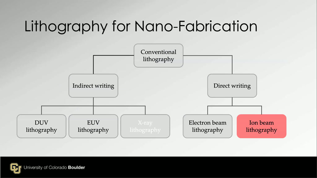
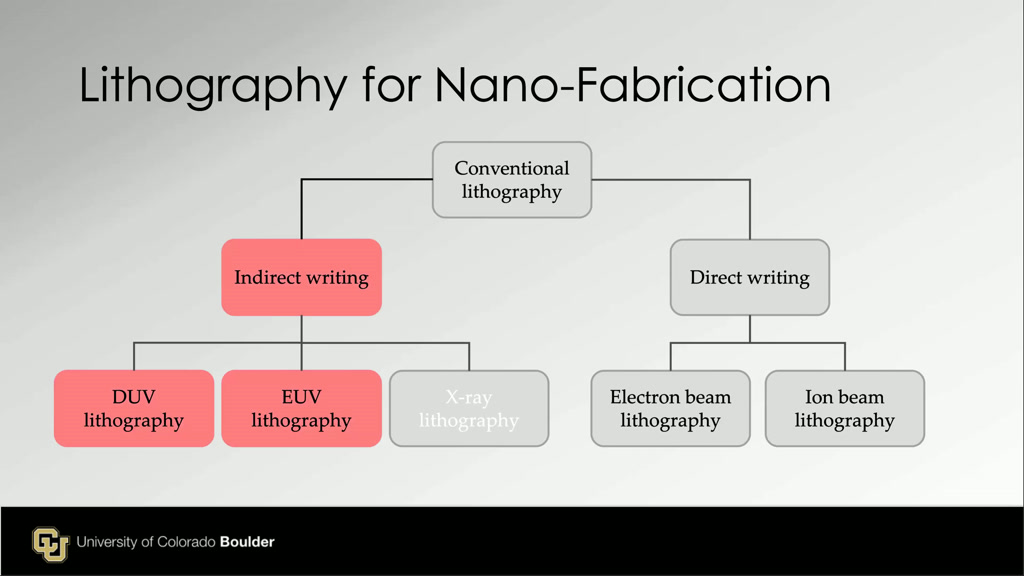 16. Lithography for Nano-Fabricati…
1663.1631631631633
00:00/00:00
16. Lithography for Nano-Fabricati…
1663.1631631631633
00:00/00:00 -
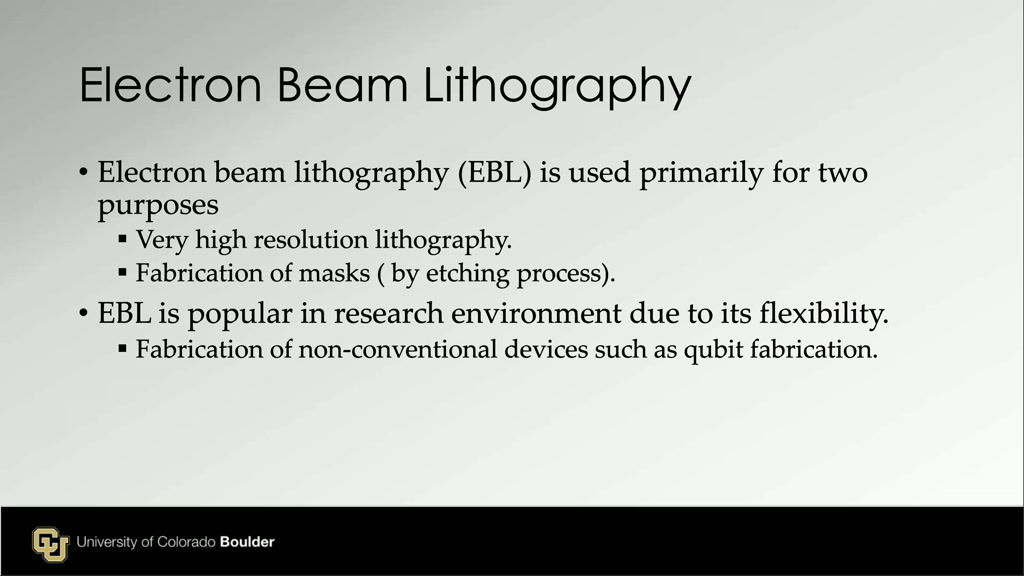 17. Electron Beam Lithography
1685.9526192859528
00:00/00:00
17. Electron Beam Lithography
1685.9526192859528
00:00/00:00 -
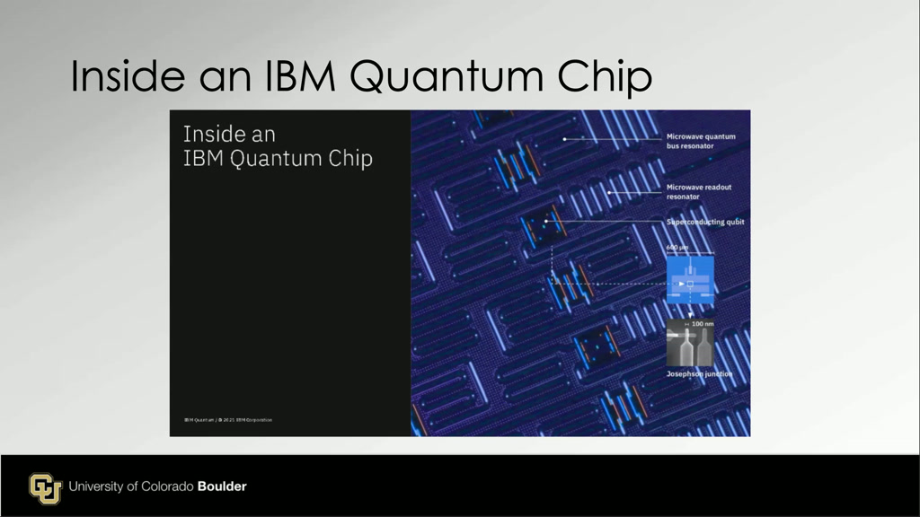 18. Inside an IBM Quantum Chip
1780.6806806806808
00:00/00:00
18. Inside an IBM Quantum Chip
1780.6806806806808
00:00/00:00 -
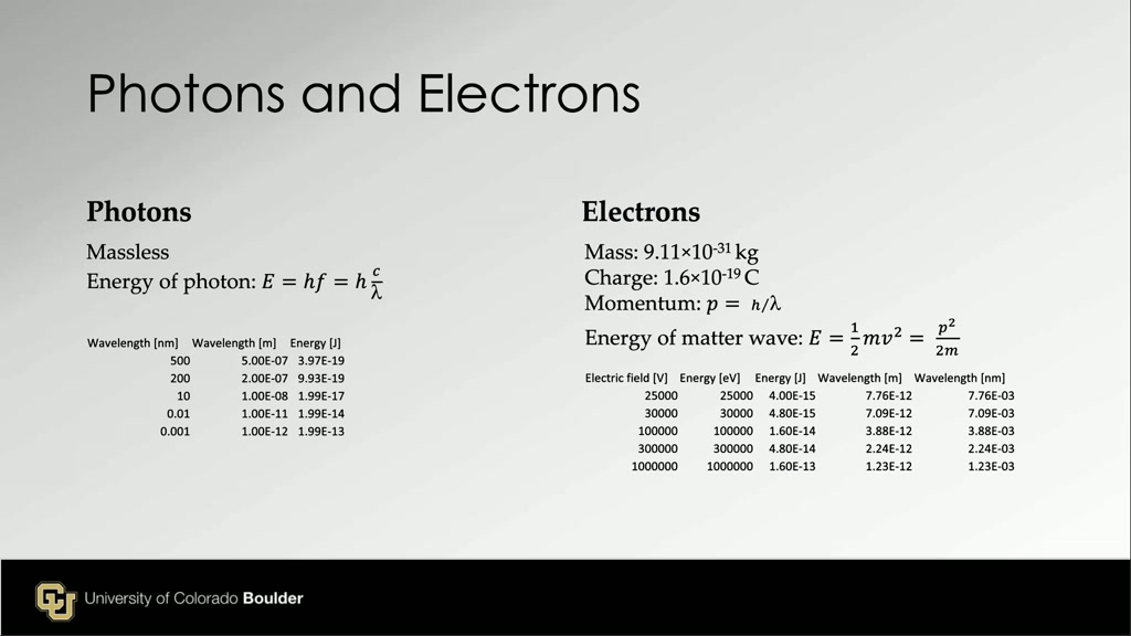 19. Photons and Electrons
1841.207874541208
00:00/00:00
19. Photons and Electrons
1841.207874541208
00:00/00:00 -
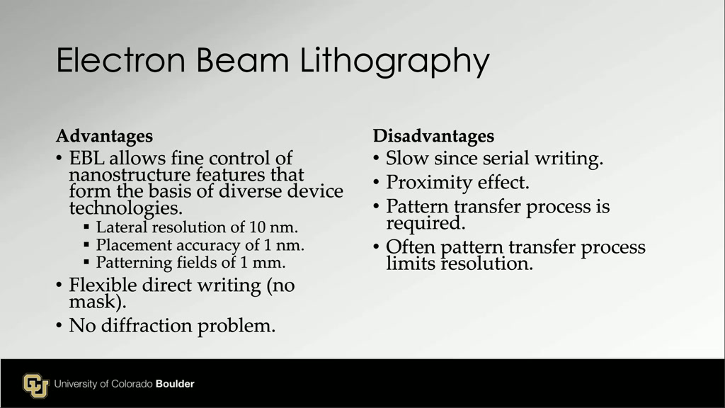 20. Electron Beam Lithography
1975.0750750750751
00:00/00:00
20. Electron Beam Lithography
1975.0750750750751
00:00/00:00 -
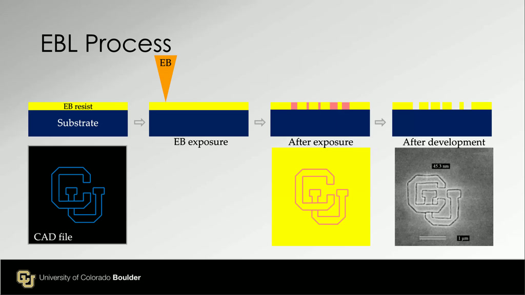 21. EBL Process
2083.5835835835837
00:00/00:00
21. EBL Process
2083.5835835835837
00:00/00:00 -
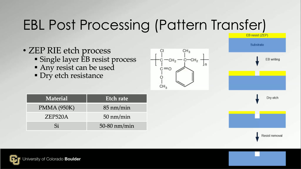
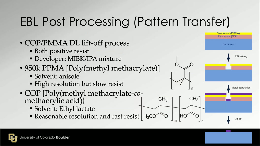 22. EBL Post Processing (Pattern T…
2228.2282282282281
00:00/00:00
22. EBL Post Processing (Pattern T…
2228.2282282282281
00:00/00:00 -
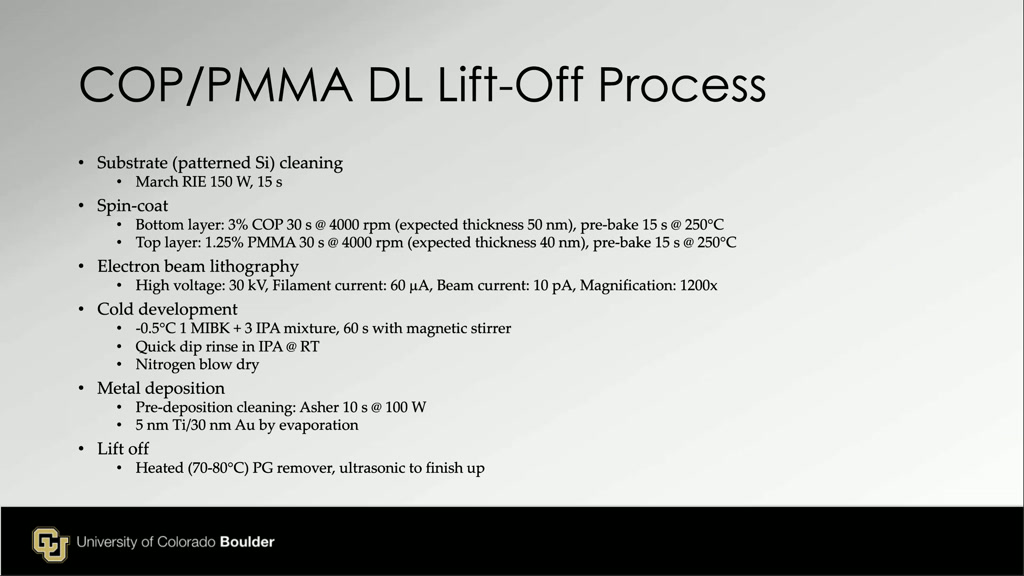 23. COP/PMMA DL Lift-Off Process
2312.0453787120455
00:00/00:00
23. COP/PMMA DL Lift-Off Process
2312.0453787120455
00:00/00:00 -
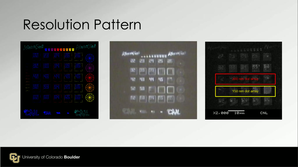 24. Resolution Pattern
2350.0500500500502
00:00/00:00
24. Resolution Pattern
2350.0500500500502
00:00/00:00 -
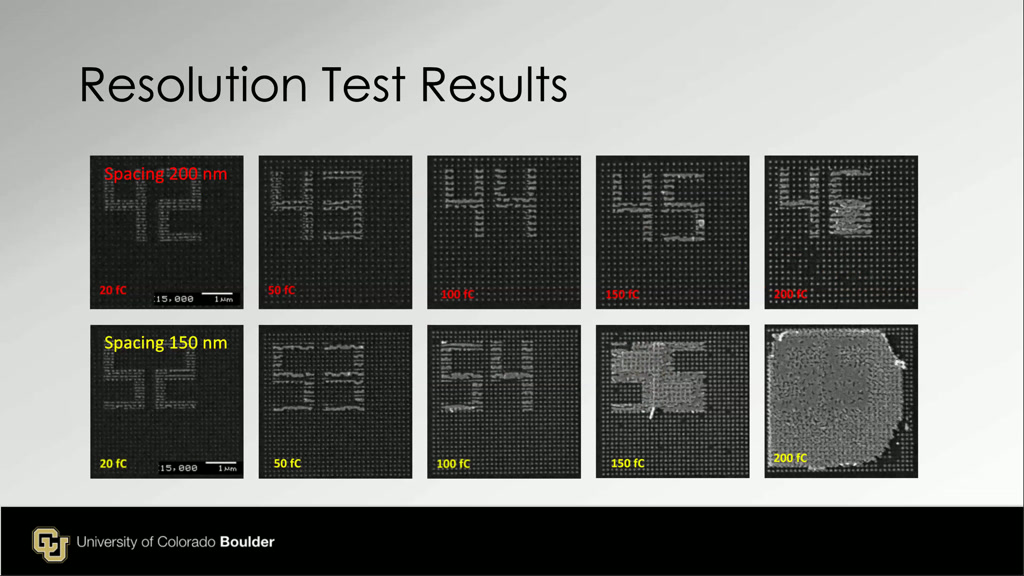 25. Resolution Test Results
2394.3943943943946
00:00/00:00
25. Resolution Test Results
2394.3943943943946
00:00/00:00 -
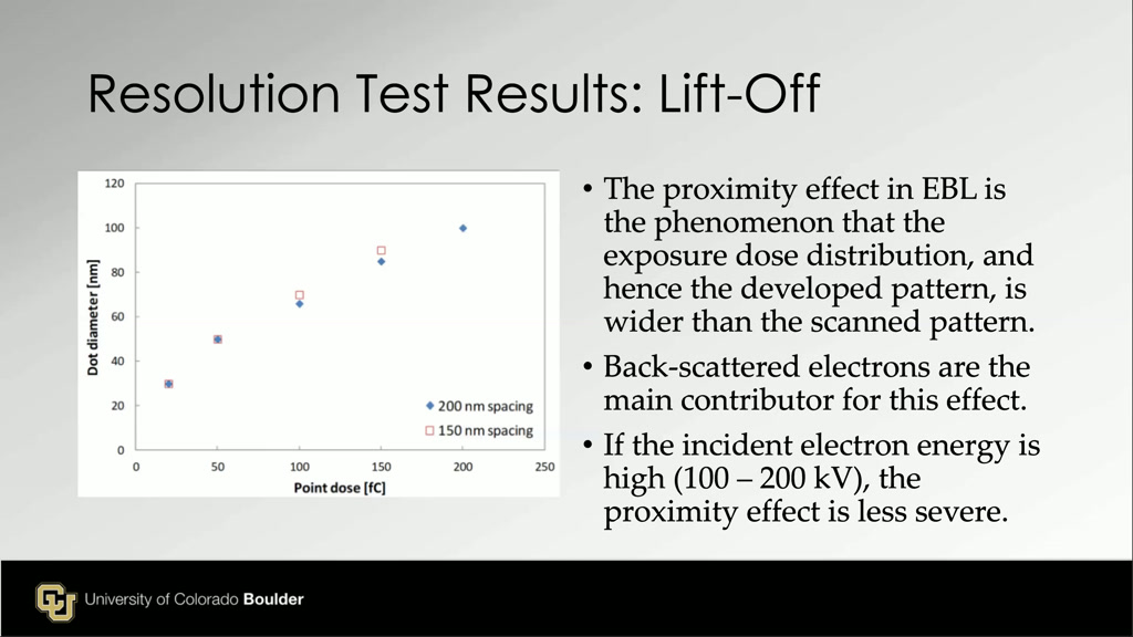 26. Resolution Test Results: Lift-…
2474.3410076743412
00:00/00:00
26. Resolution Test Results: Lift-…
2474.3410076743412
00:00/00:00 -
 27. EBL Post Processing (Pattern T…
2592.5258591925258
00:00/00:00
27. EBL Post Processing (Pattern T…
2592.5258591925258
00:00/00:00 -
 28. Zep REI Etch Process
2644.9115782449117
00:00/00:00
28. Zep REI Etch Process
2644.9115782449117
00:00/00:00 -
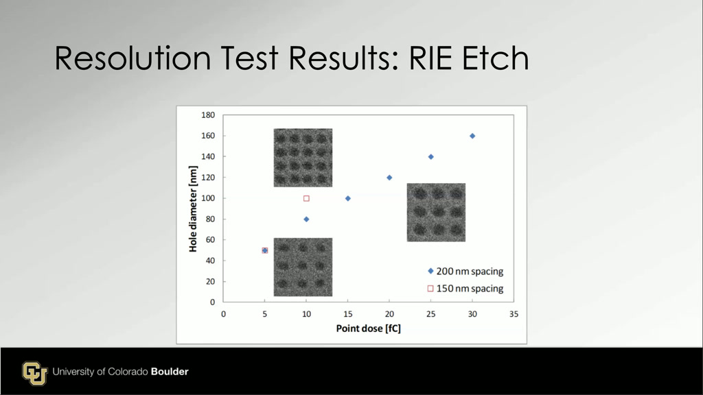 29. Resolution Test Results: RIE E…
2649.9165832499166
00:00/00:00
29. Resolution Test Results: RIE E…
2649.9165832499166
00:00/00:00 -
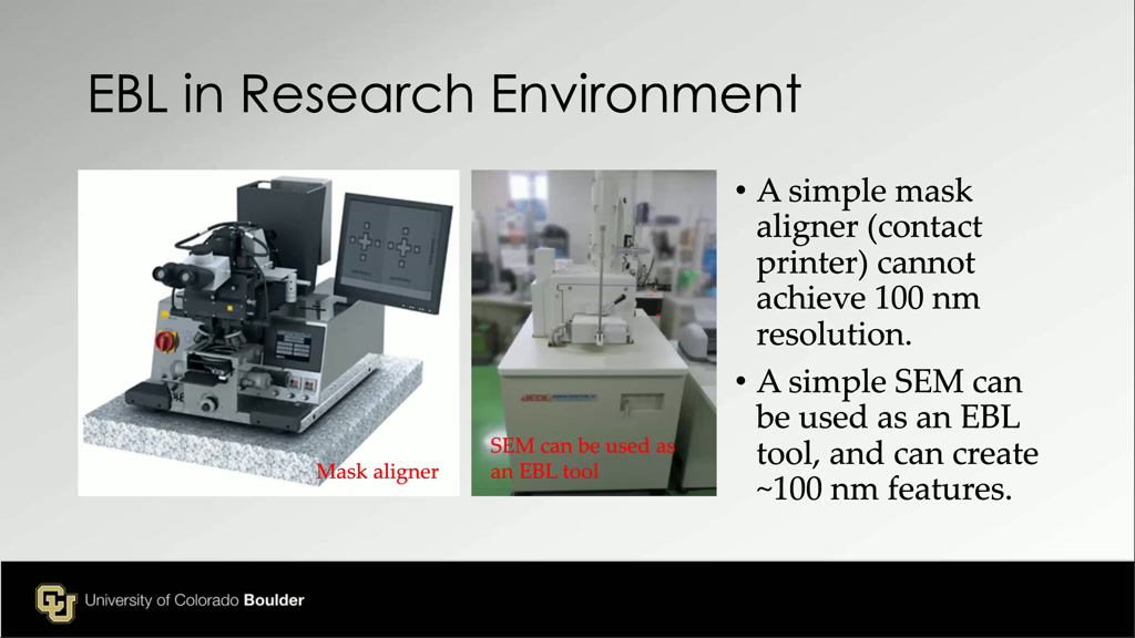 30. EBL in Research Environment
2664.0974307640977
00:00/00:00
30. EBL in Research Environment
2664.0974307640977
00:00/00:00 -
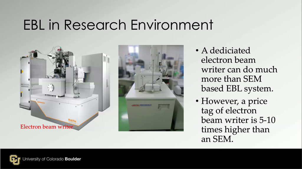 31. EBL in Research Environment
2734.6346346346349
00:00/00:00
31. EBL in Research Environment
2734.6346346346349
00:00/00:00 -
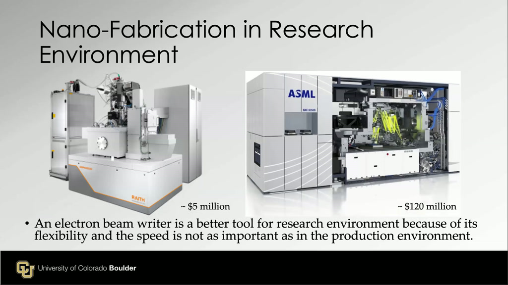 32. Nano-Fabrication in Research E…
2761.3947280613947
00:00/00:00
32. Nano-Fabrication in Research E…
2761.3947280613947
00:00/00:00 -
 33. Lithography for Nano-Fabricati…
2818.6186186186187
00:00/00:00
33. Lithography for Nano-Fabricati…
2818.6186186186187
00:00/00:00 -
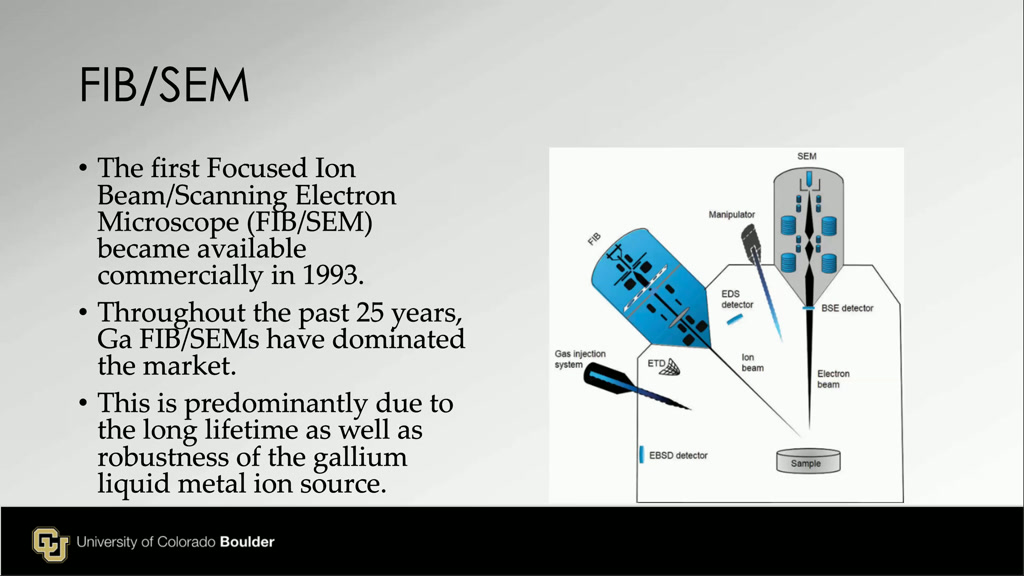 34. FIB/SEM
2837.2372372372374
00:00/00:00
34. FIB/SEM
2837.2372372372374
00:00/00:00 -
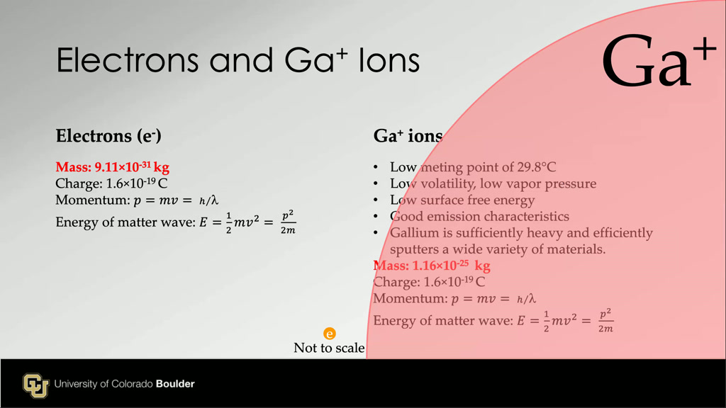 35. Electrons and Ga+ Ions
2903.5035035035035
00:00/00:00
35. Electrons and Ga+ Ions
2903.5035035035035
00:00/00:00 -
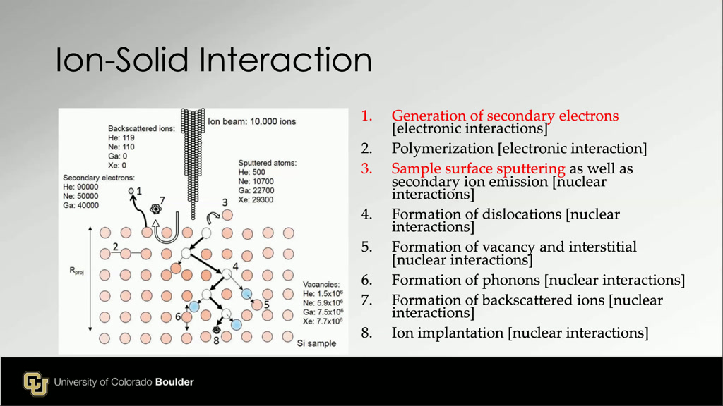 36. In-Solid Interaction
2952.7193860527195
00:00/00:00
36. In-Solid Interaction
2952.7193860527195
00:00/00:00 -
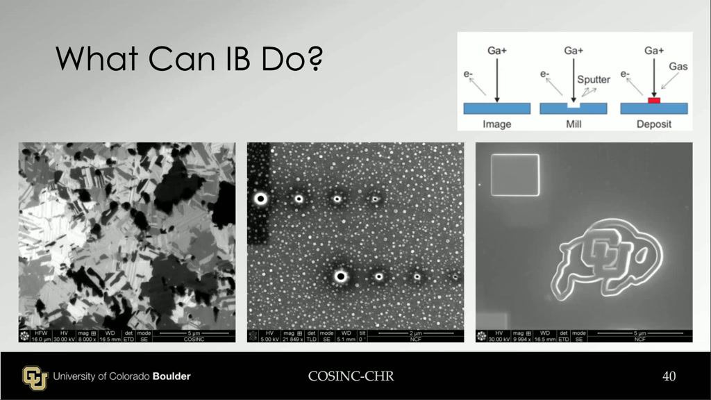 37. What can IB Do?
3069.2025358692026
00:00/00:00
37. What can IB Do?
3069.2025358692026
00:00/00:00 -
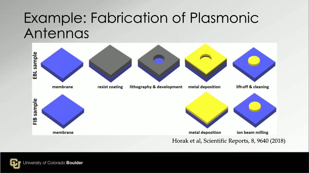 38. Examples: Fabrication of Plasm…
3189.155822489156
00:00/00:00
38. Examples: Fabrication of Plasm…
3189.155822489156
00:00/00:00 -
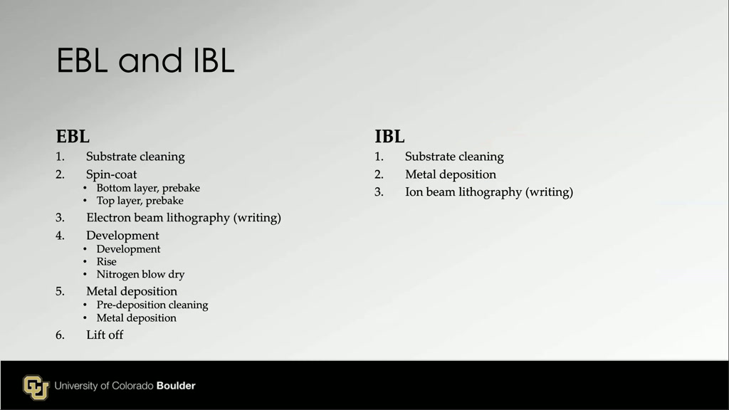 39. EBL and IBL
3238.4050717384052
00:00/00:00
39. EBL and IBL
3238.4050717384052
00:00/00:00 -
 40. EBL and IBL
3268.2015348682016
00:00/00:00
40. EBL and IBL
3268.2015348682016
00:00/00:00 -
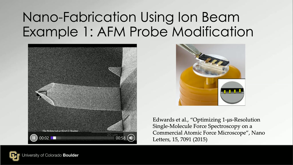 41. Example 1: AFM Probe Modificat…
3455.4888221554888
00:00/00:00
41. Example 1: AFM Probe Modificat…
3455.4888221554888
00:00/00:00 -
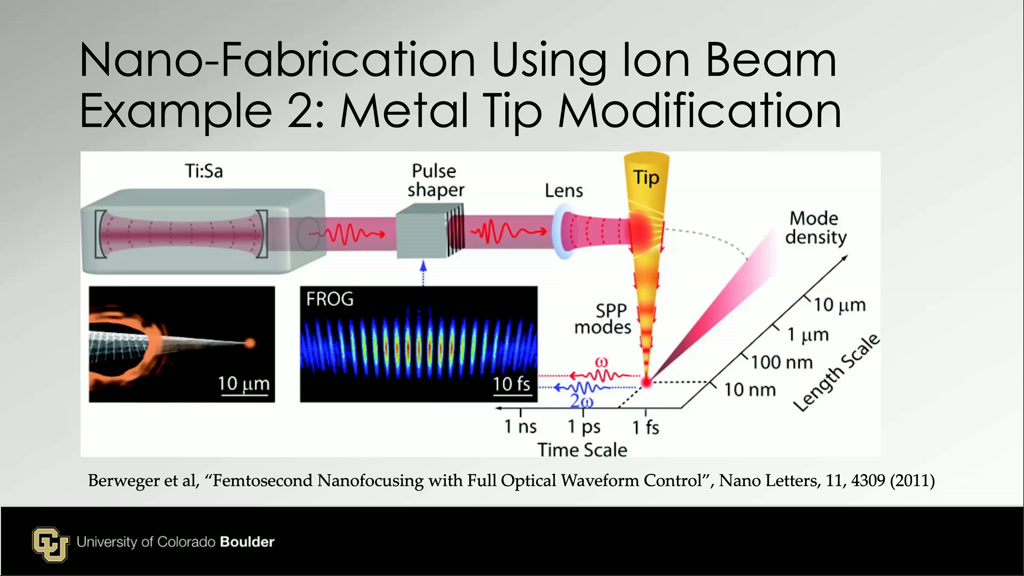 42. Example 2: Metal Tip Modificat…
3606.2395729062396
00:00/00:00
42. Example 2: Metal Tip Modificat…
3606.2395729062396
00:00/00:00 -
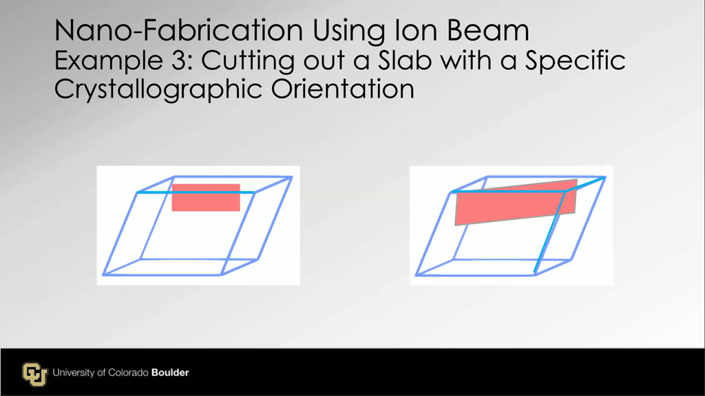 43. Example 3: Cutting out a Slab …
3669.4027360694031
00:00/00:00
43. Example 3: Cutting out a Slab …
3669.4027360694031
00:00/00:00 -
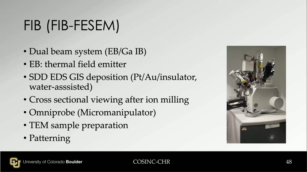 44. FIB (FIB-FESEM)
3747.6142809476146
00:00/00:00
44. FIB (FIB-FESEM)
3747.6142809476146
00:00/00:00 -
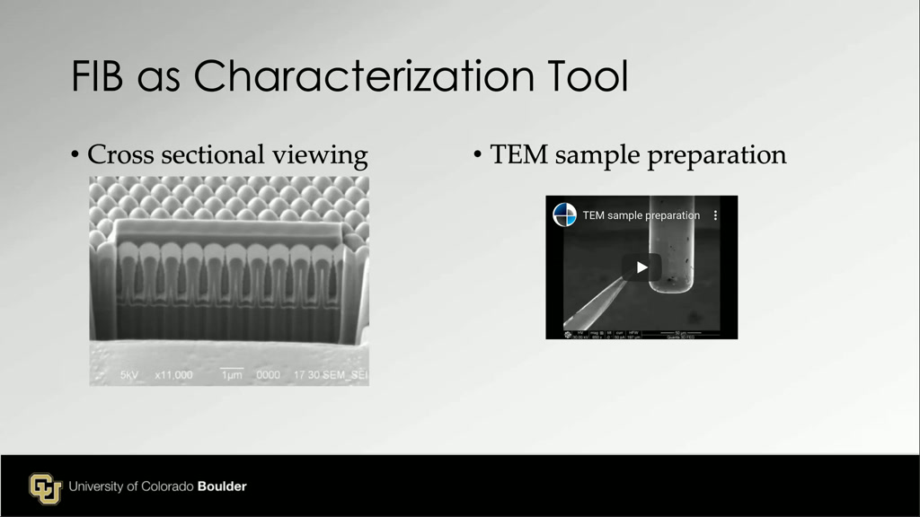 45. FIB as Characterization Tool
3807.640974307641
00:00/00:00
45. FIB as Characterization Tool
3807.640974307641
00:00/00:00 -
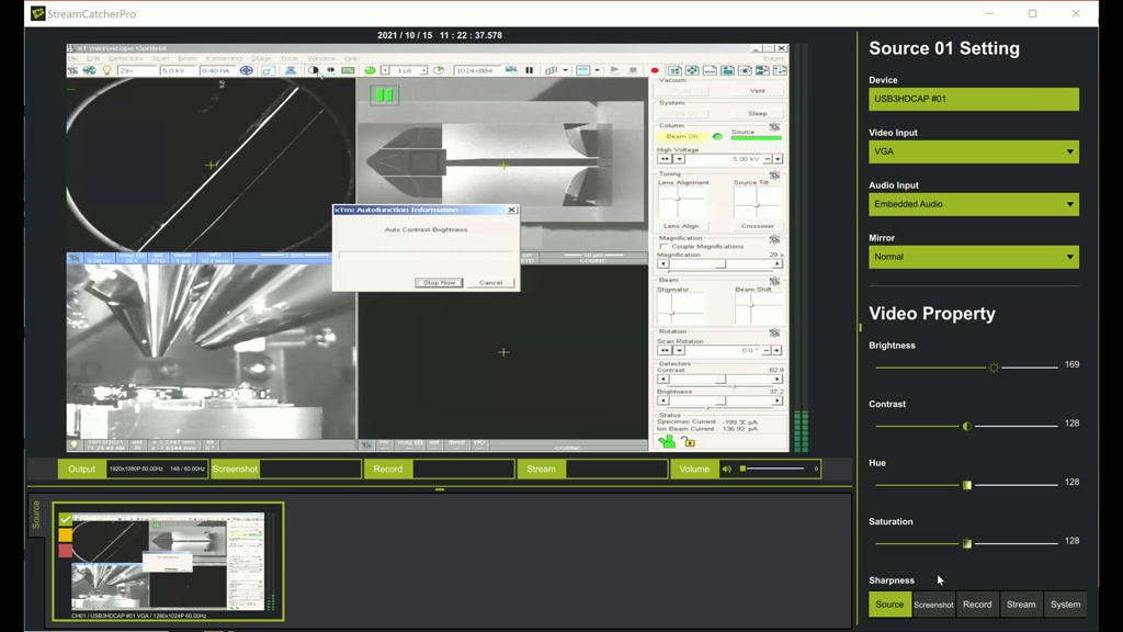 46. Demo
3935.5021688355023
00:00/00:00
46. Demo
3935.5021688355023
00:00/00:00