Introduction to Advancing Quantum Mechanics for Engineers and Physicists
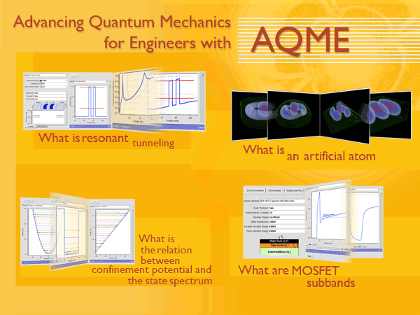
“Advancing Quantum Mechanics for Engineers” (AQME) toolbox is an assemblage of individually authored tools that, used in concert, offer educators and students a one-stop-shop for semiconductor education. The AQME toolbox holds a set of easily employable nanoHUB tools appropriate for teaching a quantum mechanics class in either engineering or physics. Users no longer have to search the nanoHUB to find the appropriate applications for discovery that are related to quantum mechanics; users, both instructors and students, can simply log in and take advantage of the assembled tools and associated materials such as homework or project assignments.
Thanks to its contributors, nanoHUB users and AQME’s toolbox have benefited tremendously from the hard work invested in tools development. Simulation runs performed using the AQME tools are credited to the individual tools, and count toward individual tool rankings. Uses of individual tools within the AQME tool set are also counted, to measure AQME impact and to improve the tool. On their respective pages, the individual tools are linked to the AQME toolbox.
Participation in this open source, interactive educational initiative is vital to its success, and all nanoHUB users can:
- Contribute content to AQME by uploading it to the nanoHUB. (See “Contribute>Contribute Content” on the nanoHUB mainpage.) Tagging contributions with “AQME” will effect an association with this initiative and, because the toolbox is actively managed, such contributions may also may be added to the toolbox.
- Provide feedback for the items you use in AQME and on nanoHUB.org through the review system. (Please be explicit and provide constructive feedback.)
- Let us know when things do not work by filing a ticket via the nanoHUB “Help” feature on every page.
- Finally, let us know what you are doing and submityour suggestions improving the nanoHUB by using the “Feedback” section, which you can find under “Support“
Finally, be sure to share AQME and other nanoHUB success stories; the nanotechnology community and its supporters need to hear of nanoHUB’s impact.
Discovery that is Possible through Quantum Mechanics
Nanotechnology has yielded a number of unique structures that are not found readily in nature. Most demonstrate an essential quality of Quantum Mechanics known as quantum confinement. Confinement is the idea of keeping electrons trapped in a small area, about 30 nm or smaller. Quantum confinement comes in several dimensions. 2-D confinement, for example, is restricted in only one dimension, resulting in a quantum well (or plane). Lasers are currently built from this dimension. 1-D confinement occurs in nanowires, and 0-D confinement is found only in the quantum dot.
The study of quantum confinement leads, foremost, to electronic properties not found in today’s semiconductor devices. The quantum dot works well as a first example. The typical quantum dot is anywhere between 3-60 nm in diameter. That’s still 30 to 600 times the size of a typical atom. A quantum dot exhibits 0-D confinement, meaning that electrons are confined in all three dimensions. In nature, only atoms have 0-D confinement; thus, a quantum dot can be described loosely as an ‘artificial atom.’ This knowledge is vitally important, as atoms are too small and too difficult to isolate in experiments. Conversely, quantum dots are large enough to be manipulated by magnetic fields and can even be moved around with an STM or AFM. We can deduce many important atomistic characteristics from a quantum dot that would otherwise be impossible to research in an atom.
Confinement also increases the efficiency of today’s electronics. The laser is based on a 2-D confinement layer that is usually created with some form of epitaxy such as Molecular Beam Epitaxy or Chemical Vapor Deposition. The bulk of modern lasers created with this method are highly functional, but these lasers are ultimately inefficient in terms of energy consumption and heat dissipation. Moving to 1-D confinement in wires or 0-D confinement in quantum dots allows for higher efficiencies and brighter lasers. Quantum dot lasers are currently the best lasers available, although their fabrication is still being worked out.
Confinement is just one manifestation of quantum mechanics in nanodevices. Tunneling and quantum interference are two other manifestations of quantum mechanics in the operation of scanning tunneling microscopes and resonant tunneling diodes, respectively. For more information on the theoretical aspects of Quantum Mechanics check the following resources:
Quantum Mechanics for Engineers
Quantum Mechanics for Engineers: Course Assignments
Because understanding quantum mechanics is so foundational to an understanding of the operation of nanoscale devices, almost every Electrical Engineering department (in which there is a strong nanotechnology experimental or theoretical group) and all Physics departments teach the fundamental principles of quantum mechanics and their application to nanodevice research. Several conceptual sets and theories are taught within these courses. Normally, students are first introduced to the concept of particle-wave duality (the photoelectric effect and the double-slit experiment), the solutions of the time-independent Schrödinger equation for open systems (piece-wise constant potentials), tunneling, and bound states. The description of the solution of the Schrödinger equation for periodic potentials (Kronig-Penney model) naturally follows from the discussion of double well, triple well and n-well structures. This leads the students to the concept of energy bands and energy gaps, and the concept of the effective mass that can be extracted from the pre-calculated band structure by fitting the curvature of the bands. The Tsu-Esaki formula is then investigated so that, having calculated the transmission coefficient, students can calculate the tunneling current in resonant tunneling diode and Esaki diode. After establishing basic principles of quantum mechanics, the harmonic oscillator problem is then discussed in conjunction with understanding vibrations of a crystalline lattice, and the idea of phonons is introduced as well as the concept of creation and annihilation operators. The typical quantum mechanics class for undergraduate/first-year graduate students is then completed with the discussion of the stationary and time-dependent perturbation theory and the derivation of the Fermi Golden Rule, which is used as a starting point of a graduate level class in semiclassical transport. Coulomb Blockade is another discussion a typical quantum mechanics class will include.
Particle-Wave Duality
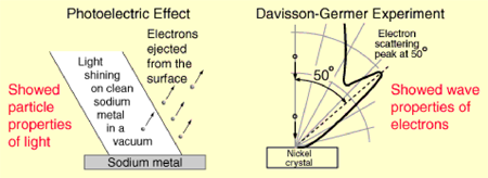 A wave-particle dual nature was discovered and publicized in the early debate about whether light was composed of particles or wave. Evidence for the description of light-as-waves was well established at the turn of the century when the photoelectric effect introduced firm evidence of a light-as-particle nature. This dual nature was found to also be characteristic of electrons. Electron particle nature properties were well documented when the DeBroglie hypothesis, and subsequent experiments by Davisson and Germer, established the wave nature of the electron.
Particle-Wave Duality: an Animation
This movie helps students to better distinguish when nano-things behave as particles and when they behave as waves. The link below connects to an exercise on these concepts.
Introductory Concepts in Quantum Mechanics: an Exercise
Solution of the Time-Independent Schrödinger Equation
Piece-Wise Linear Barrier Tool in AQME – Open Systems


The Piece-Wise Linear Barrier Tool in AQME allows calculation of the transmission and the reflection coefficient of arbitrary five, seven, nine, eleven and 2n-segment piece-wise constant potential energy profile. For the case of multi-well structure it also calculates the quasi-bound states so it can be used as a simple demonstration tool for the formation of energy bands. Also, it can be used in the case of stationary perturbation theory exercises to test the validity of, for example, the first order and the second order correction to the ground state energy of the system due to small perturbations of, for example, the confining potential. The Piece-Wise Linear Barrier Tool in AQME can also be used to test the validity of the WKB approximation for triangular potential barriers.
Available resources:
- Quantum-Mechanical Reflections: an Exercise
- Double-Barrier Case: An Exercise
- From 1 well to 2 wells to 5 wells to periodic potentials: an Exercise
- Energy Bands as a Function of the Geometry of the n-Well Potential: an Exercise
- Cosine Bands: an Exercise for PCPBT
- Quantum-Mechanical Reflections in Nanodevices: an Exercise
- Tunneling Through Triangular Barrier: an Exercise for PCPBT
- Stationary Perturbation Theory: an Exercise for PCPBT
Bound States Lab in AQME
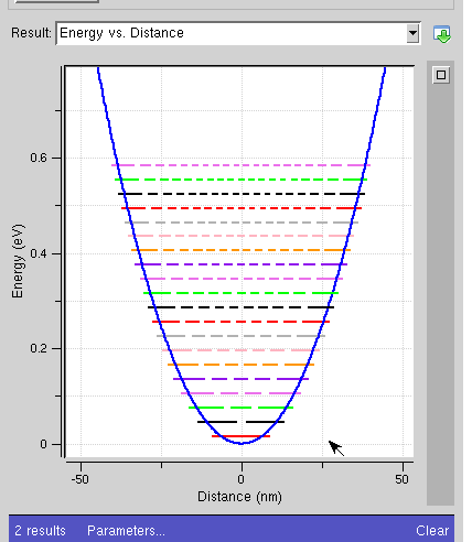
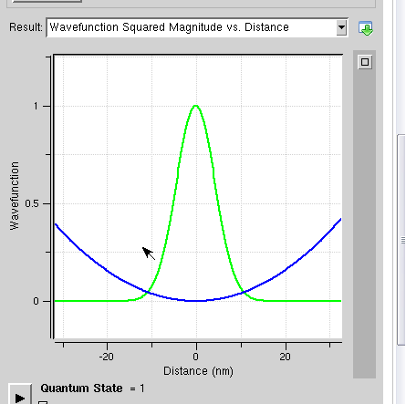
The Bound States Lab in AQME determines the bound states and the corresponding wavefunctions in a square, harmonic, and triangular potential well. The maximum number of eigenstates that can be calculated is 100. Students clearly see the nature of the separation of the states in these three prototypical confining potentials, with which students can approximate realistic quantum potentials that occur in nature.
The panel below (left) shows energy eigenstates of a harmonic oscillator. Probability density of the ground state that demonstrates purely quantum-mechanical behavior is shown in the middle panel below. Probability density of the 20th subband demonstrates the more classical behavior as the well opens (right panel below).

Available resources:
Energy Bands and Effective Masses
Periodic Potential Lab in AQME
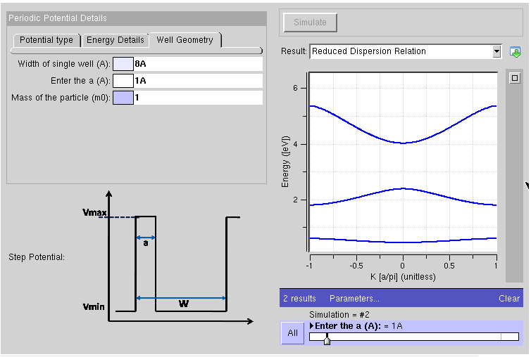
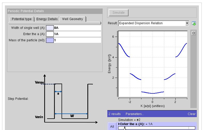 The Periodic Potential Lab in AQME solves the time-independent Schrödinger Equation in a 1-D spatial potential variation. Rectangular, triangular, parabolic (harmonic), and Coulomb potential confinements can be considered. The user can determine energetic and spatial details of the potential profiles, compute the allowed and forbidden bands, plot the bands in a compact and an expanded zone, and compare the results against a simple effective mass parabolic band. Transmission is also calculated. This lab also allows the students to become familiar with the reduced zone and expanded zone representation of the dispersion relation (E-k relation for carriers).
Available resources:
Periodic Potentials and Bandstructure: an Exercise
Band Structure Lab in AQME
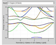
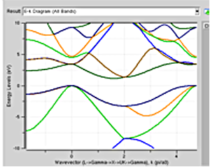 Band structure of Si (left panel) and GaAs (right panel).
In solid-state physics, the electronic band structure (or simply band structure) of a solid describes ranges of energy that an electron is “forbidden” or “allowed” to have. It is due to the diffraction of the quantum mechanical electron waves in the periodic crystal lattice. The band structure of a material determines several characteristics, in particular, its electronic and optical properties. The Band Structure Lab in AQME enables the study of bulk dispersion relationships of Si, GaAs, InAs. Plotting the full dispersion relation of different materials, students first get familiar with a band structure of a direct band gap (GaAs, InAs), as well as indirect band gap semiconductors (Si). For the case of multiple conduction band valleys, students must first determine the Miller indices of one of the equivalent valleys, then, from that information they can deduce how many equivalent conduction bands are in Si and Ge, for example. In advanced applications, the users can apply tensile and compressive strain and observe the variation in the band structure, band gaps, and effective masses. Advanced users can also study band structure effects in ultra-scaled (thin body) quantum wells, and nanowires of different cross sections. Band Structure Lab uses the sp3s*d5 tight-binding method to compute E(k) for bulk, planar, and nanowire semiconductors.
Available resource:
Bulk Band Structure: a Simulation Exercise
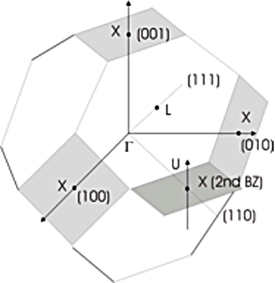 The figure on the left illustrates the first Brillouin zone of FCC lattice that corresponds to the first Brillouin zone for all diamond and Zinc-blende materials (C, Si, Ge, GaAs, InAs, CdTe, etc.). There are 8 hexagonal faces (normal to 111) and 6 square faces (normal to 100). The sides of each hexagon and each square are equal.
Supplemental Information: Specification of High-Symmetry Points
| Symbol | Description |
| Γ | Center of the Brillouin zone |
| Simple Cube | |
| M | Center of an edge |
| R | Corner point |
| X | Center of a face |
| Face-Centered Cubic | |
| K | Middle of an edge joining two hexagonal faces |
| L | Center of a hexagonal face |
| U | Middle of an edge joining a hexagonal and a square face |
| W | Corner point |
| X | Center of a square face |
| Body-Centered Cubic | |
| H | Corner point joining four edges |
| N | Center of a face |
| P | Corner point joining three edges |
| Hexagonal | |
| A | Center of a hexagonal face |
| H | Corner point |
| K | Middle of an edge joining two rectangular faces |
| L | Middle of an edge joining a hexagonal and a rectangular face |
| M | Center of a rectangular face |
Real World Applications
Schred Tool in AQME

The Schred Tool in AQME calculates the envelope wavefunctions and the corresponding bound-state energies in a typical MOS (Metal-Oxide-Semiconductor) or SOS (Semiconductor-Oxide- Semiconductor) structure and in a typical SOI structure by solving self-consistently the one-dimensional (1-D) Poisson equation and the 1D Schrödinger equation. The Schred tool is specifically designed for Si/SiO2 interface and takes into account the mass anisotropy of the conduction bands, as well as different crystallographic orientations.
Available resources:
 Right panel – Potential diagram for inversion of p-type semiconductor. In this first notation Εij refers to the j-th subband from either the Δ2-band (i=1) or Δ4-band (i=2). Left panel – Constant-energy surfaces for the conduction-band of silicon showing six conduction-band valleys in the direction of momentum space. The band minima, corresponding to the centers of the ellipsoids, are 85% of the way to the Brillouin-zone boundaries. The long axis of an ellipsoid corresponds to the longitudinal effective mass of the electrons in silicon, while the short axes correspond to the transverse effective mass . For orientation of the surface, the Δ2-band has the longitudinal mass (ml) perpendicular to the semiconductor interface and the Δ4-band has the transverse mass (mt) perpendicular to the interface. Since larger mass leads to smaller kinetic term in the Schrodinger equation, the unprimed lader of subbands (as is usually called), corresponding to the Δ2-band, has the lowest ground state energy. The degeneracy of the unprimed ladder of subbands for orientation of the surface is 2. For the same reason, the ground state of the primed ladder of subbands corresponding to the Δ4-band is higher that the lowest subband of the unprimed ladder of subbands, The degeneracy of the primed ladder of subbands for (100) orientation of the interface is 4.
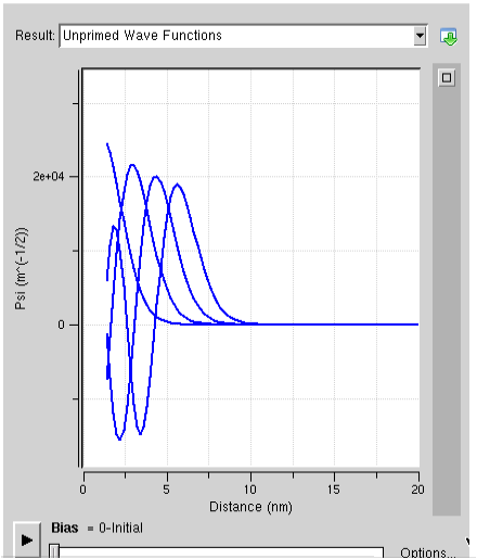
1-D Heterostructure Tool AQME
The 1-D Heterostructure Tool AQME simulates confined states in 1-D heterostructures by calculating charge self-consistently in the confined states, based on a quantum mechanical description of the one dimensional device. The greater interest in HEMT devices is motivated by the limits that will be reached with scaling of conventional transistors. The 1D Heterostructure Tool in that respect is a very valuable tool for the design of HEMT devices as one can determine, for example, the position and the magnitude of the delta-doped layer, the thickness of the barrier and the spacer layer for which one maximizes the amount of free carriers in the channel which, in turn, leads to larger drive current. This is clearly illustrated in the examples below.


Available resources:
- Uniform versus delta doping in 1D heterostructures: an Exercise
- Parallel Conduction Channel: an Exercise for 1D Heterostructure Lab
The most commonly used semiconductor devices for applications in the GHz range now are GaAs based MESFETs, HEMTs and HBTs. Although MESFETs are the cheapest devices because they can be realized with bulk material, i.e. without epitaxially grown layers, HEMTs and HBTs are promising devices for the near future. The advantage of HEMTs and HBTs is a factor of 2 to 3 higher power density compared to MESFETs which leads to significantly smaller chip size.
HEMTs are field effect transistors where the current flow between two ohmic contacts, Source and Drain, and it is controlled by a third contact, the Gate. Most often the Gate is a Schottky contact. In contrast to ion implanted MESFETs, HEMTs are based on epitaxially grown layers with different band gaps Eg. A schematic cross section of a HEMT is shown below.
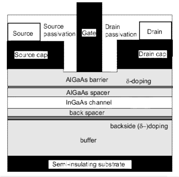 Schematic cross section of a High Electron Mobility Transistor (HEMT).
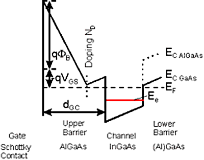 If two semiconductors with different band gap energies are joined together, the difference is divided up into a band gap offset in the valence band ΔEV and a band gap offset in the conduction band ΔEC. One of the most common assumptions made for the AlGaAs/InGaAs material system is 40% valence band offset and 60% conduction band offset. This is only valid for Al contents below about 45%. For higher Al contents the bandgap of AlGaAs changes from direct to indirect. In the figure below such an AlGaAs/InGaAs HEMT with a delta doped upper barrier layer is shown. The conduction band energy under the gate along the cutting line A-A’ is shown to the right.
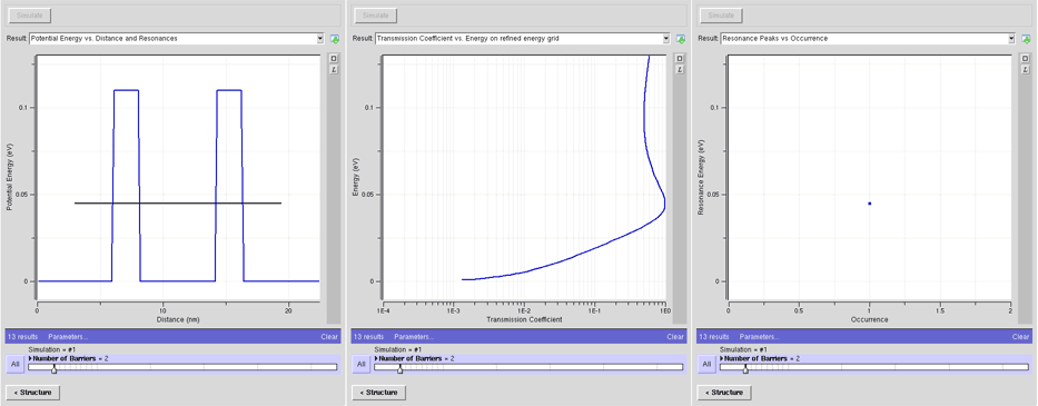
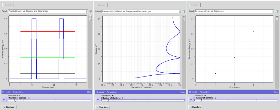
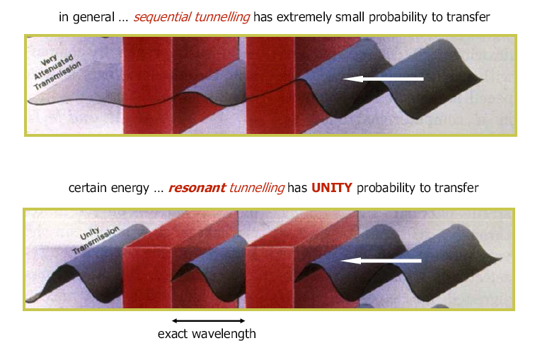
Resonant Tunneling Diode Lab in AQME


Put a potential barrier in the path of electrons, and it will block their flow; but, if the barrier is thin enough, electrons can tunnel right through due to quantum mechanical effects. It is even more surprising that, if two or more thin barriers are placed closely together, electrons will bounce between the barriers, and, at certain resonant energies, flow right through the barriers as if there were none. Run the Resonant Tunneling Diode Lab in AQME, which lets you control the number of barriers and their material properties, and then simulate current as a function of bias. Devices exhibit a surprising negative differential resistance, even at room temperature. This tool can be run online in your web browser as an active demo.
Available resources:
Quantum Dot Lab in AQME
Individual quantum dots can be created from two-dimensional electron or hole gases present in remotely doped quantum wells or semiconductor heterostructures. The sample surface is coated with a thin layer of resist. A lateral pattern is then defined in the resist by electron beam lithography. This pattern can then be transferred to the electron or hole gas by etching, or by depositing metal electrodes (lift-off process) that allow the application of external voltages between the electron gas and the electrodes. Such quantum dots are mainly of interest for experiments and applications involving electron or hole transport, i.e., an electrical current. The energy spectrum of a quantum dot can be engineered by controlling the geometrical size, the shape, and the strength of the confinement potential. Also, in contrast to atoms, it is relatively easy to connect quantum dots by tunnel barriers to conducting leads, which allows the application of the techniques of tunneling spectroscopy for their investigation. Confinement in quantum dots can also arise from electrostatic potentials (generated by external electrodes, doping, strain, or impurities).
 Quantum Dot Lab in AQME computes the eigenstates of a particle in a box of various shapes, including domes and pyramids.
Available resources:
- Quantum Dots is a nano 101, introductory lecture that starts from particle-wave duality and explores the concepts of quantum dots.
- Introduction to Quantum Dot Lab (by Lee, Ryu, Klimeck)
- Quantum Dot Lab Learning Module: An Introduction (by Fodor, Guo)
- Quantum Dot Spectra, Absorption, and State Symmetry: an Exercise
Scattering and Fermi’s Golden Rule

Scattering is a general physical process whereby some forms of radiation, such as light, sound, or moving particles are forced to deviate from a straight trajectory by one or more localized non-uniformities in the medium through which they pass. In conventional use, scattering also includes deviation of reflected radiation from the angle predicted by the law of reflection. Reflections that undergo scattering are often called diffuse reflections, and unscattered reflections are called specular (mirror-like) reflections. The types of non-uniformities (sometimes known as scatterers or scattering centers) that can cause scattering are too numerous to list, but a small sample includes particles, bubbles, droplets, density fluctuations in fluids, defects in crystalline solids, surface roughness, cells in organisms, and textile fibers in clothing. The effects of such features on the path of almost any type of propagating wave or moving particle can be described in the framework of scattering theory. In quantum physics, Fermi’s golden rule is a way to calculate the transition rate (probability of transition per unit time) from one energy eigenstate of a quantum system into a continuum of energy eigenstates, due to a perturbation. The Bulk Monte-Carlo Lab in AQME calculates the scattering rates dependence versus electron energy of the most important scattering mechanisms for the most commonly used materials in the semiconductor industry, such as Si, Ge, GaAs, InSb, GaN, SiC. For proper parameter set for, for example, 4H SiC please refer to the following article.
Available Resources:
- Time-Dependent Perturbation Theory: an Exercise
- Bulk Monte Carlo Lab:Scattering Rates for Parabolic vs. Non-Parabolic Bands: an Exercise
Coulomb Blockade
In physics, a Coulomb blockade, named after Charles-Augustin de Coulomb, is the increased resistance at small bias voltages of an electronic device comprising at least one low-capacitance tunnel junction. According to the laws of classical electrodynamics, no current can flow through an insulating barrier. According to the laws of quantum mechanics, however, there is a non-vanishing (larger than zero) probability for an electron on one side of the barrier to reach the other side. When a bias voltage is applied, this means that there will be a current flow. In first-order approximation, that is, neglecting additional effects, the tunneling current will be proportional to the bias voltage. In electrical terms, the tunnel junction behaves as a resistor with a constant resistance, also known as an ohmic resistor. The resistance depends exponentially on the barrier thickness. Typical barrier thicknesses are on the order of one to several nanometers. An arrangement of two conductors with an insulating layer in between not only has a resistance, but also a finite capacitance. The insulator is also called dielectric in this context, the tunnel junction behaves as a capacitor.

The Coulomb Blockade Lab in AQME allows simulation of non-linear current-voltage (I-V) characteristics through single and double quantum dots and as such illustrates various single electron transport phenomena.
Available resources:
- Coulomb Blockade Exercises
- Coulomb blockade design exercises that uses Quantum Dot Lab
Users no longer have to search the nanoHUB to find the appropriate applications for discovery that are related to quantum mechanics; users, both instructors and students, can simply log in to the AQME toolbox and take advantage of the assembled tools and resources, such as animations, exercises or podcasts.