ECE 695Q Lecture 01: Introduction
ECE 695Q Lecture 01: Introduction
-
 1. Nanometer Scale Patterning and…
0
00:00/00:00
1. Nanometer Scale Patterning and…
0
00:00/00:00 -
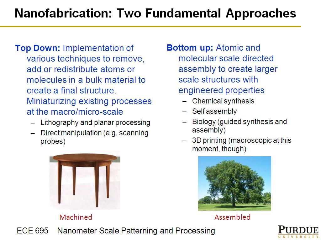
 2. Nanometer Scale Patterning and…
29.195862529195864
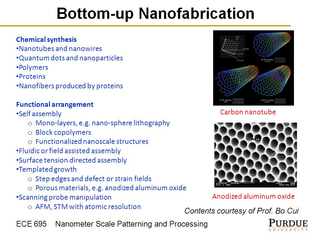
00:00/00:00
2. Nanometer Scale Patterning and…
29.195862529195864
00:00/00:00 -
 3. About the course
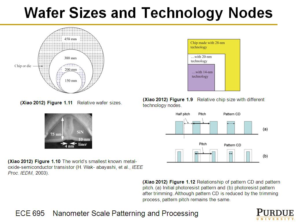
59.392726059392729
00:00/00:00
3. About the course
59.392726059392729
00:00/00:00 -
 4. Major References
152.85285285285286
00:00/00:00
4. Major References
152.85285285285286
00:00/00:00 -
 5. Assignments, Expectations and …
195.8958958958959
00:00/00:00
5. Assignments, Expectations and …
195.8958958958959
00:00/00:00 -
 6. Tentative Schedule
289.65632298965636
00:00/00:00
6. Tentative Schedule
289.65632298965636
00:00/00:00 -
 7. Tentative Schedule (Continued)
316.48314981648315
00:00/00:00
7. Tentative Schedule (Continued)
316.48314981648315
00:00/00:00 -
 8. Nanotechnology/Nanostructures:…
334.40106773440107
00:00/00:00
8. Nanotechnology/Nanostructures:…
334.40106773440107
00:00/00:00 -
 9. Nanofabrication: Two Fundament…
445.34534534534538
00:00/00:00
9. Nanofabrication: Two Fundament…
445.34534534534538
00:00/00:00 -
 10. Example of a Bottom-Up Fabrica…
560.82749416082754
00:00/00:00
10. Example of a Bottom-Up Fabrica…
560.82749416082754
00:00/00:00 -
 11. Bottom-up Nanofabrication
793.32665999332664
00:00/00:00
11. Bottom-up Nanofabrication
793.32665999332664
00:00/00:00 -
 12. Top-Down Nanofab: Semiconducto…
934.70136803470143
00:00/00:00
12. Top-Down Nanofab: Semiconducto…
934.70136803470143
00:00/00:00 -
 13. How are Chips made?
1006.7067067067068
00:00/00:00
13. How are Chips made?
1006.7067067067068
00:00/00:00 -
 14. Brief History of Semiconductor…
1140.1067734401067
00:00/00:00
14. Brief History of Semiconductor…
1140.1067734401067
00:00/00:00 -
 15. Integrated Circuits
1319.386052719386
00:00/00:00
15. Integrated Circuits
1319.386052719386
00:00/00:00 -
 16. Wafer Sizes and Technology Nod…
1339.4728061394728
00:00/00:00
16. Wafer Sizes and Technology Nod…
1339.4728061394728
00:00/00:00 -
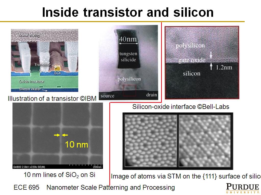 17. Inside transistor and silicon
1681.2479145812479
00:00/00:00
17. Inside transistor and silicon
1681.2479145812479
00:00/00:00 -
 18. Inside an integrated circuit c…
1740.5071738405072
00:00/00:00
18. Inside an integrated circuit c…
1740.5071738405072
00:00/00:00 -
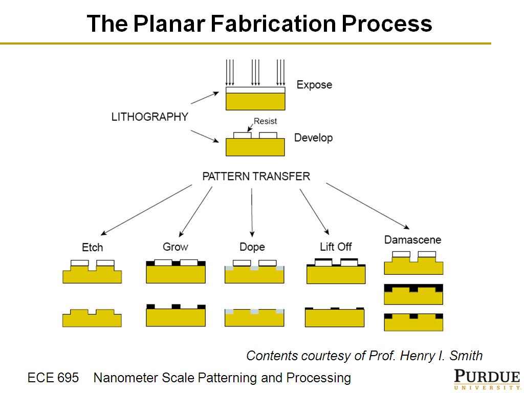 19. The Planar Fabrication Process
1811.4781448114782
00:00/00:00
19. The Planar Fabrication Process
1811.4781448114782
00:00/00:00 -
 20. Layer-by-layer approach to 3D …
2221.9552886219553
00:00/00:00
20. Layer-by-layer approach to 3D …
2221.9552886219553
00:00/00:00 -
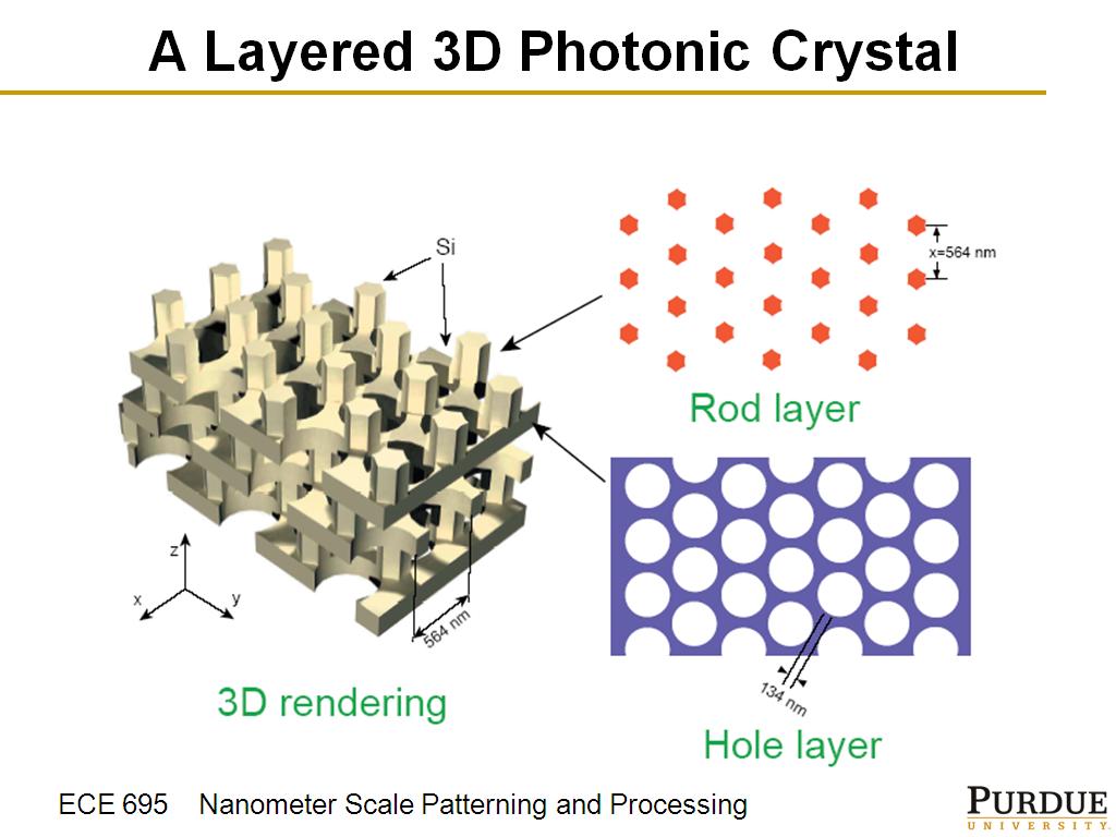 21. A Layered 3D Photonic Crystal
2319.5528862195529
00:00/00:00
21. A Layered 3D Photonic Crystal
2319.5528862195529
00:00/00:00 -
 22. Aligned Nanostructures
2337.5709042375711
00:00/00:00
22. Aligned Nanostructures
2337.5709042375711
00:00/00:00 -
 23. Cross-Sectional View
2356.0894227560893
00:00/00:00
23. Cross-Sectional View
2356.0894227560893
00:00/00:00 -
 24. Anatomy of a CMOS Transistor
2371.6049382716051
00:00/00:00
24. Anatomy of a CMOS Transistor
2371.6049382716051
00:00/00:00 -
 25. Example: Layout and Binary Mas…
2863.8304971638304
00:00/00:00
25. Example: Layout and Binary Mas…
2863.8304971638304
00:00/00:00