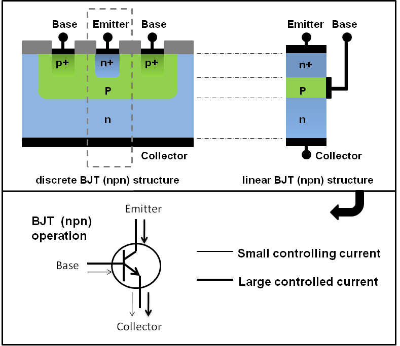
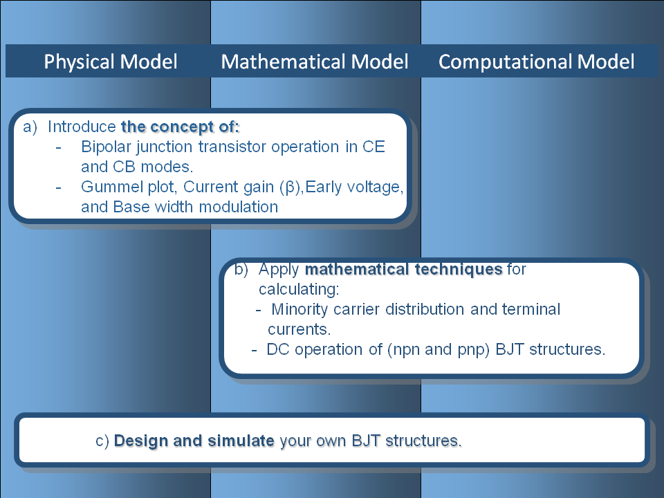
By completing the BJT Lab in ABACUS - Assembly of Basic Applications for Coordinated Understanding of Semiconductors, users will be able to understand a) BJT (Bipolar Junction Transistor) operation (npn and pnp type) in Common Emitter and Common Base modes, and b) the concept of early voltage, base width modulation and Gummel Plot. Users will also learn how to design and study their own BJT structures.
The specific objectives of the BJT Lab are:
Recommended Reading
Users who are new to the operation of BJT should consult the following resources:
Rober F. Pierret. (1996). Semiconductor Device Fundamentals. Reading, MA: Addison-Wesley. (See especially chapters 10-11)
Demo
BJT Lab: First-Time User Guide
Theoretical Descriptions
* Tutorial_PADRE_Simulation_Tools.pdf (tutorial)
* Illinois ECE 440 Solid State Electronic Devices, Lecture 25: Intro to BJT
* Illinois ECE 440 Solid State Electronic Devices, Lecture 26: Narrow-base BJT
* Illinois ECE 440 Solid State Electronic Devices, Lecture 27: BJT Gain
* Illinois ECE 440 Solid State Electronic Devices, Lecture 28&29: All Modes of BJT Operation
* ECE 606 Lecture 27: Introduction to Bipolar Transistors (Graduate level)
* ECE 606 Lecture 28: BJT Design I (Graduate level)
* ECE 606 Lecture 29: BJT Design II (Graduate level)
Tool Verification
* Verification of the Validity of the BJT Tool
Examples
1. BJT Lab Worked Out Problem 1
2. BJT Lab Worked Out Problem 2
Exercises and Homework Assignments
1. BJT Problems and PADRE Exercise
3. Homework Exercise on Bipolar Junction Transistors
Solutions to Exercises
Solutions are provided only to instructors!