Electron Density in a Nanowire
Category
Published on
Abstract
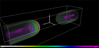 Electron Density in a circular Silicon nanowire transistor. The left and the right regions on the image represent the large electron densities in the source and drain of the transistor. The central section represents the gated region that enables the control of the electron flow through the nano-scale on-off switch.
Continued down-scaling of transistors have enabled the tremendous advances in consumer electronics. We are reaching the limits where the individual transistors or on-off electron valves are only a few nanometers in diameters wide. At these atomic length scales the electrons do no longer act like billiard balls but like waves. Sophisticated modeling engines that consider a quantum mechanical description of the electrons, an atomistic description of the material, and non-equilibrium electron distributions are needed for device design and optimization.
The "Nanowire" tool on nanoHUB.org enables such device modeling and enables the visualization of the electron density in such ultra-scaled structures through 3D volume rendering.
Credits
Purdue University
References
- Nanoelectronic Modeling:
Gerhard Klimeck and Mathieu Luisier, "Atomistic Modeling of Realistically Extended Semiconductor Devices with NEMO/OMEN," IEEE Computing in Science and Engineering (CISE) Vol.12, pg. 28-35 (2010). (available on nanoHUB.org) - nanoVIZ:
Wei Qiao, Michael Mclennan, Rick Kennell, David Ebert, and Gerhard Klimeck, "Hub-based Simulation and Graphics Hardware Accelerated Visualization for Nanotechnology Applications", IEEE Transactions on Visualization and Computer Graphics, Vol. 12, pg. 1061-1068 (2006). - nanoHUB.org:
Alejandro Strachan, Gerhard Klimeck, Mark S. Lundstrom, "Cyber-Enabled Simulations in Nanoscale Science and Engineering", Computing in Science and Engineering, Vol. 12, pg: 12-17 (2010). (available on nanoHUB.org) - Nanowire tool on nanoHUB.org:
Hong-Hyun Park, Lang Zeng, Matthew Buresh, Siqi Wang, Gerhard Klimeck, Saumitra Raj Mehrotra, Clemens Heitzinger, Benjamin P Haley, Jay Mashl (2010), "Nanowire", DOI: 10254/nanohub-r1307.7.
Cite this work
Researchers should cite this work as follows: