MOSCap

By Akira Matsudaira1; Saumitra Raj Mehrotra2; Shaikh S. Ahmed3; Gerhard Klimeck2; Dragica Vasileska4

1. University of Illinois at Urbana-Champaign 2. Purdue University 3. Southern Illinois University Carbondale 4. Arizona State University

Capacitance of a MOS device

Launch Tool

You must login before you can run this tool.

Version 1.8 - published on 23 Jul 2014

doi:10.4231/D3736M30D cite this

This tool is closed source.

First-Time User Guide View All Supporting Documents

    SCREENSHOT #1 SCREENSHOT #2 CV profile with different oxide thickness Surface Potential Vs Vg SCREENSHOT #5 DEMO #1

Category

Tools

Published on

Abstract

    The primary reason to study Metal-Oxide-Silicon (MOS) capacitors is to understand the principle of operation as well as the detailed analysis of the Metal-Oxide-Silicon Field Effect Transistor(MOSFET). 
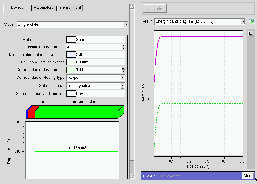
MOSCap simulates the one-dimensional electrostatics in typical single and dual-gate Metal-Oxide-Semiconductor device structures along the growth direction as a function of device size, geometry, oxide charge, temperature, doping concentration, and applied frequency. Among the quantities simulated, the low and high-frequency capacitance-voltage (CV) characteristics and various spatial profiles (e.g., energy band, vertical electric field, charge densities etc.) are of special importance. MOSCap also has an option for Surface Potential plot. It analytically gives the relation between applied gate potential and the semiconductor surface potential.
    To better understand the operation of a MOS capacitor, we provide brief tutorials and some typical exercises. These resources are meant to help increase comprehension of the operation of MOS capacitors from a semi-classical viewpoint. For a quantum-mechanical description of the charge in a MOS capacitor channel, please use the SCHRED tool.
  • Tutorial on MOS capacitors operation
  • Tutorial on MOS capacitors modeling with PADRE
  • Exercises for MOS capacitors that utilize PADRE
  • Theoretical Exercise for MOS Capacitors
  • CV curves and charges in the oxide and at the semiconductor/oxide interface
    • MOSCap is based on the Padre simulation tool developed by Mark Pinto, R. Kent Smith, and Ashraful Alam at Bell Labs.
      Improvements / modifications in subsequent version releases:
  • 1.7 - Added Surface Potential Vs Gate Bias plot for PADRE based results.
  • 1.6.2 - Fixed for not overwriting previous runs.
  • 1.6.1 - Default parameter set restored to 0.1um thick oxide thickness,; Tau=1ns.
  • 1.6 - Fixed phim definition for different gate materials.
  • 1.5 - Meshing made more robust for convergence. Bias stepping made finer for low frequency CV curve near threshold voltage.
  • 1.4.3 - Separated - PADRE based C-V calculations and Analytical Surface Potential plot to run independently.
  • 1.4.2 - Fixed for error in sign of Interface trap and Oxide charge densities.
  • 1.4.1 - Improved mesh density.
  • 1.4 - Added Surface Potential plot option. Input deck modified for AC frequency and carrier lifetimes.
  • 1.3 - Added the reference line for (Oxide Capacitance) Cox and interface trap charge in output plots.
  • 1.2 - Added interface charge density in input deck.
  • 1.1 - Updated work function (PHIms) definition. Input is now work function difference
  • 1.0 - MOSCapacitor simulator launched.
  • Powered by

    PADRE (Pisces And Device REplacement) developed by Mark Pinto at AT&T Bell Labs.

    Cite this work

    Researchers should cite this work as follows:

    • Akira Matsudaira, Saumitra Raj Mehrotra, Shaikh S. Ahmed, Gerhard Klimeck, Dragica Vasileska (2014), "MOSCap," https://nanohub.org/resources/moscap. (DOI: 10.4231/D3736M30D).

      BibTex | EndNote

    Tags